TSH11 데이터 시트보기 (PDF) - STMicroelectronics
부품명
상세내역
제조사
TSH11 Datasheet PDF : 6 Pages
| |||
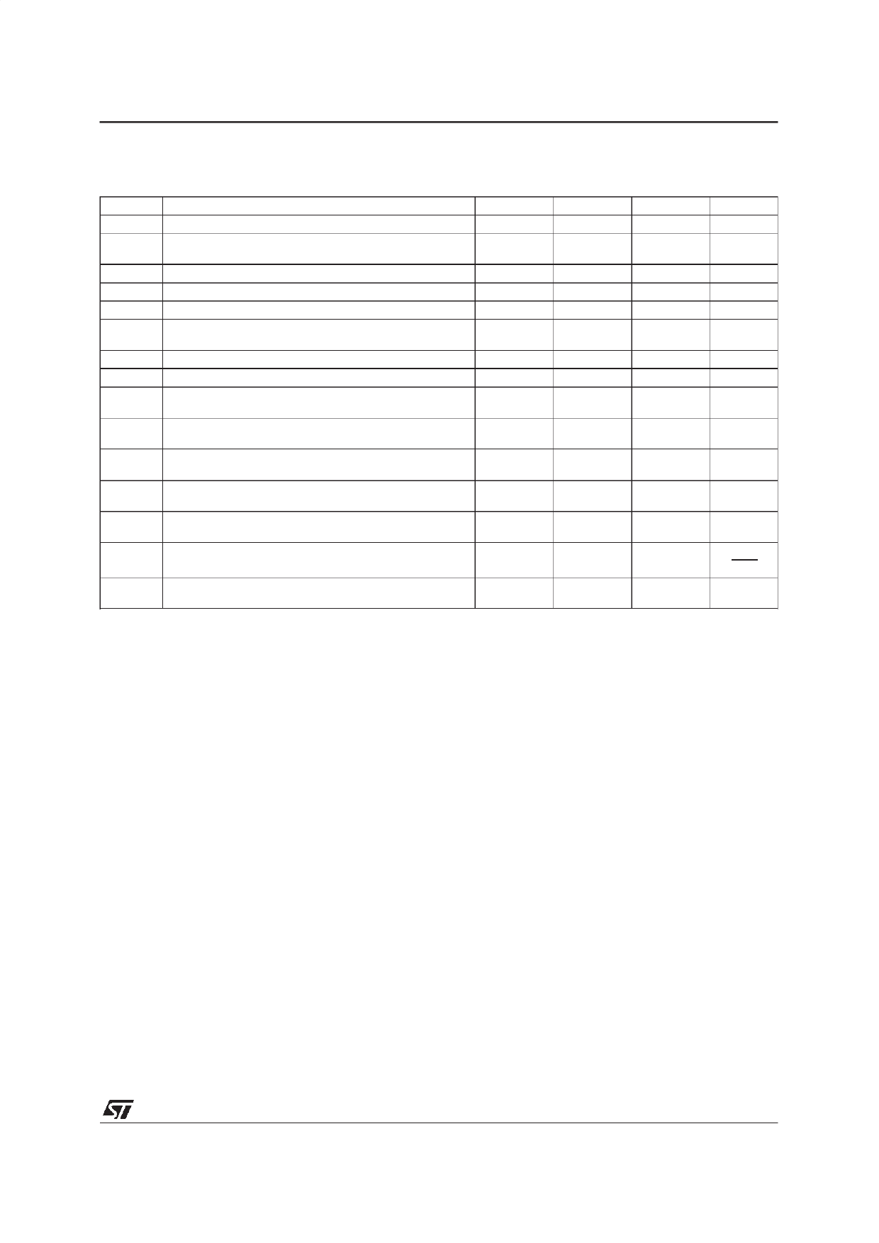
ELECTRICAL CHARACTERISTICS
VCC = ± 5V, Tamb = 25oC (unless otherwise specified)
Symbol
Vio
DVio
Iib
Iio
ICC
Avd
Vicm
CMR
SVR
Vo
Parameter
Input Offset Voltage
Input Offset Voltage Drift
Tmin ≤ Tamb ≤ Tmax
Input Bias Current
Input Offset Current
Supply Current, no load
Large Signal Voltage Gain
Vo = ±2.5V
VCC = ± 5V
RL= 100Ω
Input Common Mode Voltage Range
Common Mode Rejection Ratio Vic = Vicm min.
Supply Voltage Rejection Ratio
VCC = ± 5V to ± 3V
Output Voltage
RL = 100Ω
Io
GBP
SR
en
∅m
Output Short Circuit Current
Vid = ±1V, Vo = 0V
Gain Bandwidth Product
AVCL = 100, RL = 100Ω, f = 7.5MHz
Slew Rate
Vin = ± 2V, AVCL = 1, RL = 100Ω
Equivalent Input Voltage Noise f = 1MHz
Phase Margin
AVM = 1, RL = 100Ω, CL = 15pF
TSH11
Min.
200
-5 to +2
55
45
± 2.5
Typ.
3
20
2
2
20
800
-5.5 to +2.5
95
65
+3.5
-3.7
±70
120
150
20
Max.
15
300
200
40
40
Unit
mV
µV/oC
pA
pA
mA
V/V
V
dB
dB
V
mA
MHz
V/µs
nV
√Hz
Degrees
3/6
Share Link: 