NT3965 데이터 시트보기 (PDF) - Novatek Microelectronics
부품명
상세내역
제조사
NT3965 Datasheet PDF : 12 Pages
| |||
NT3965
TFT LCD Source Driver
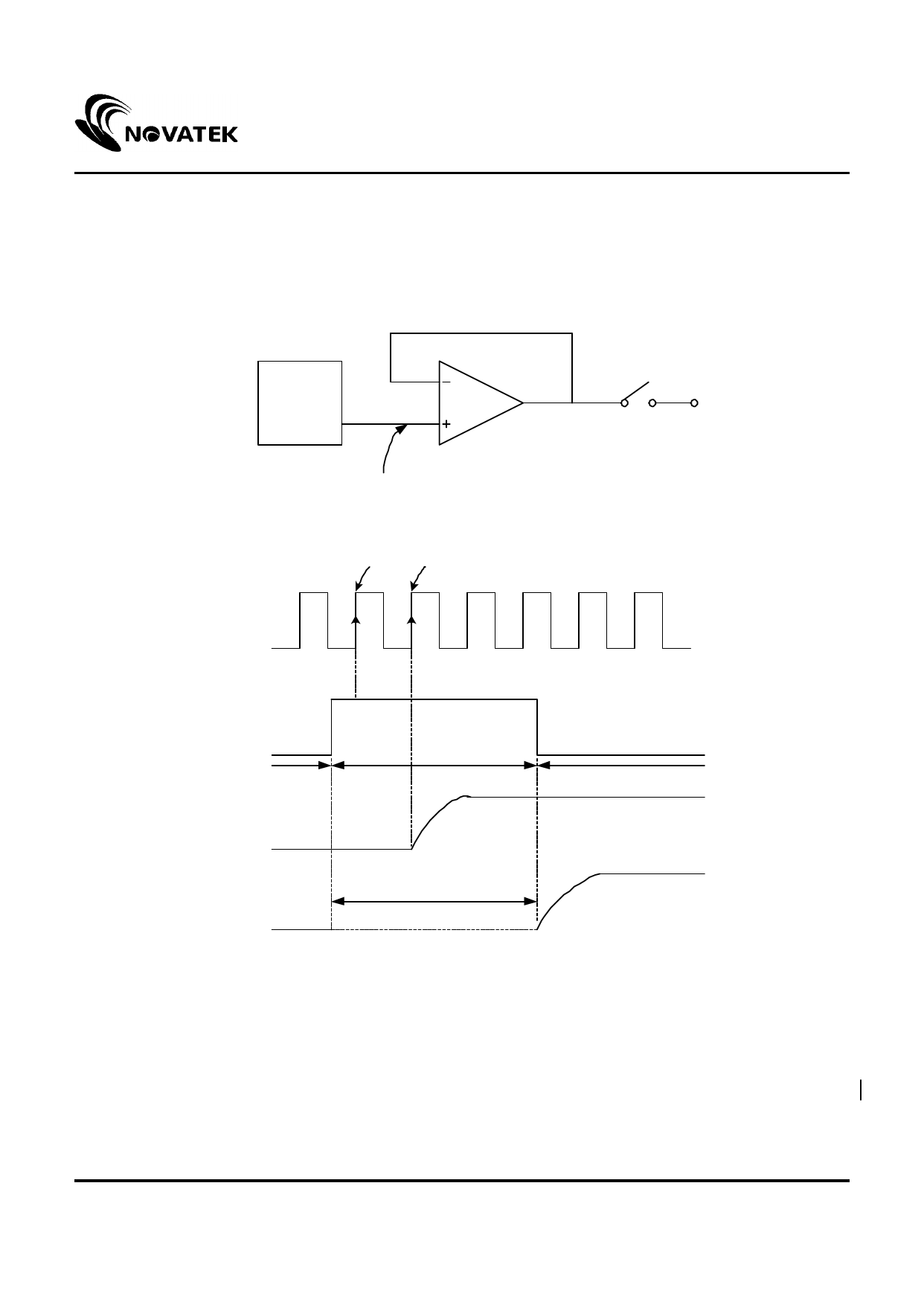
Application notice: relationship between LD, CLK, and output waveform
The output voltage is written to the LCD panel, and synchronized with the LD falling edge.
Output Circuit Block
Diagram
DAC
Vamp (in)
Output
Amp
Output Circuit Timing
Waveform
(1)
(2)
CLK
Vout
SW
LD
SW: ON
SW: OFF
SW: ON
Vamp(in)
Vout
High-Z
Remarks: 1. LD = "L" : SW = ON
LD = "H" : SW = OFF
2. LD = "H" is acknowledged at timing (1)
3. The display data latch is completed at timing (2) and the input voltage
(Vamp(in) : gray-scale level voltage) of the output amplifier changes.
12
Version 2.0
Share Link: 