DSP56156 데이터 시트보기 (PDF) - Motorola => Freescale
부품명
상세내역
제조사
DSP56156 Datasheet PDF : 76 Pages
| |||
Freescale Semiconductor, Inc.
Introduction
Pin Groupings
Pin Groupings
The DSP56156 is available in a 112-pin Ceramic Quad Flat Pack (CQFP) and a 112-pin Plastic
Thin Quad Flat Pack (TQFP). The input and output signals are organized into the functional
groups indicated in Table 3. Figure 2 illustrates the chip’s pin functions.
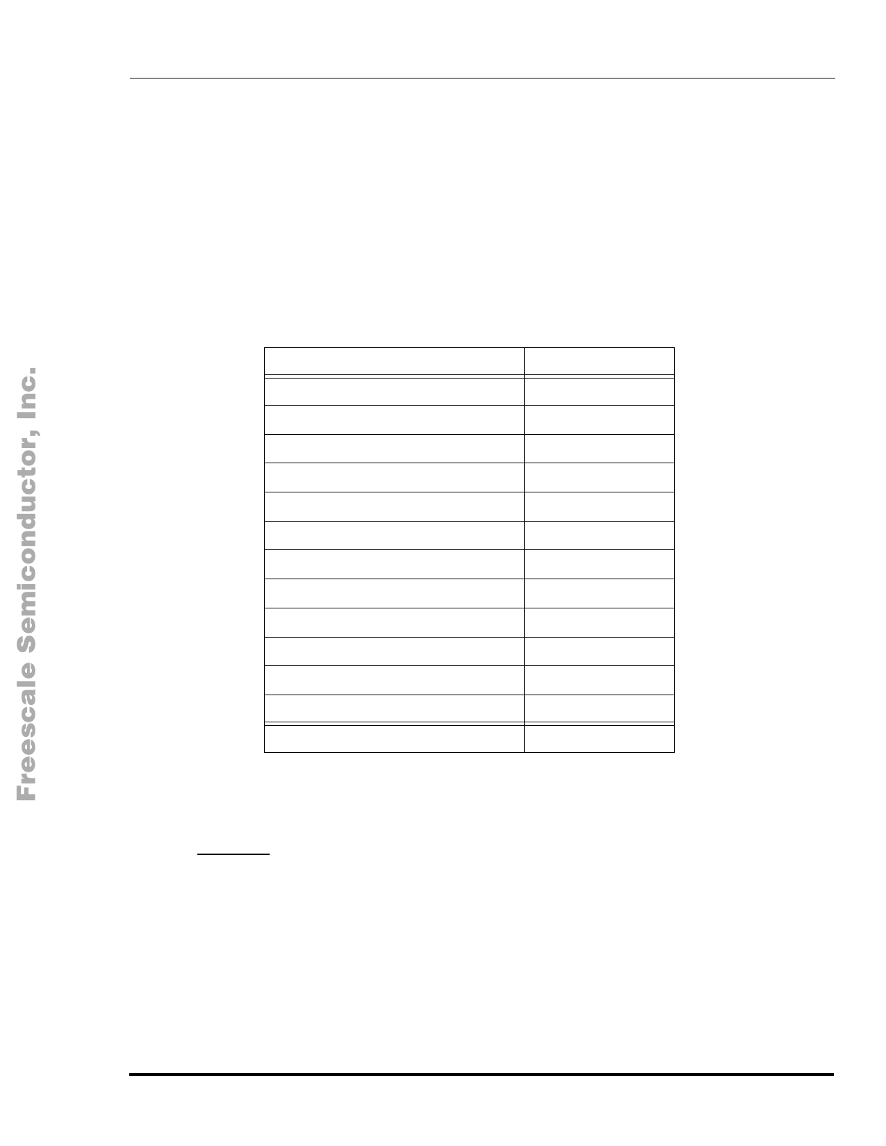
Table 3 Functional Pin Groupings
Functional Group
Address
Data Bus
Bus Control
Host Interface (HI)
Synchronous Serial Interfaces (SSI)
Timer Interface
Interrupt and Mode Control
Phase-Locked Loop (PLL) and Clock
On-Chip Emulation (OnCETM Port)
On-Chip Codec
Power (VCC)
Ground (GND)
Total
Number of Pins
16
16
9
15
10
2
4
3
4
7
10
16
112
NOTE:
OVERBARS are used throughout this document to indicate a signal which is at Ground voltage (typi-
cally a TTL logic low — VIL or VOL) when the function is logically true. These signals are, likewise, at
VCC voltage (typically a TTL logic high — VIH or VOH) when the function is logically false.
MOTOROLA
DSP56156 Data Sheet
5
For More Information On This Product,
Go to: www.freescale.com
Share Link: 