M28W320CT 데이터 시트보기 (PDF) - STMicroelectronics
부품명
상세내역
제조사
M28W320CT Datasheet PDF : 42 Pages
| |||
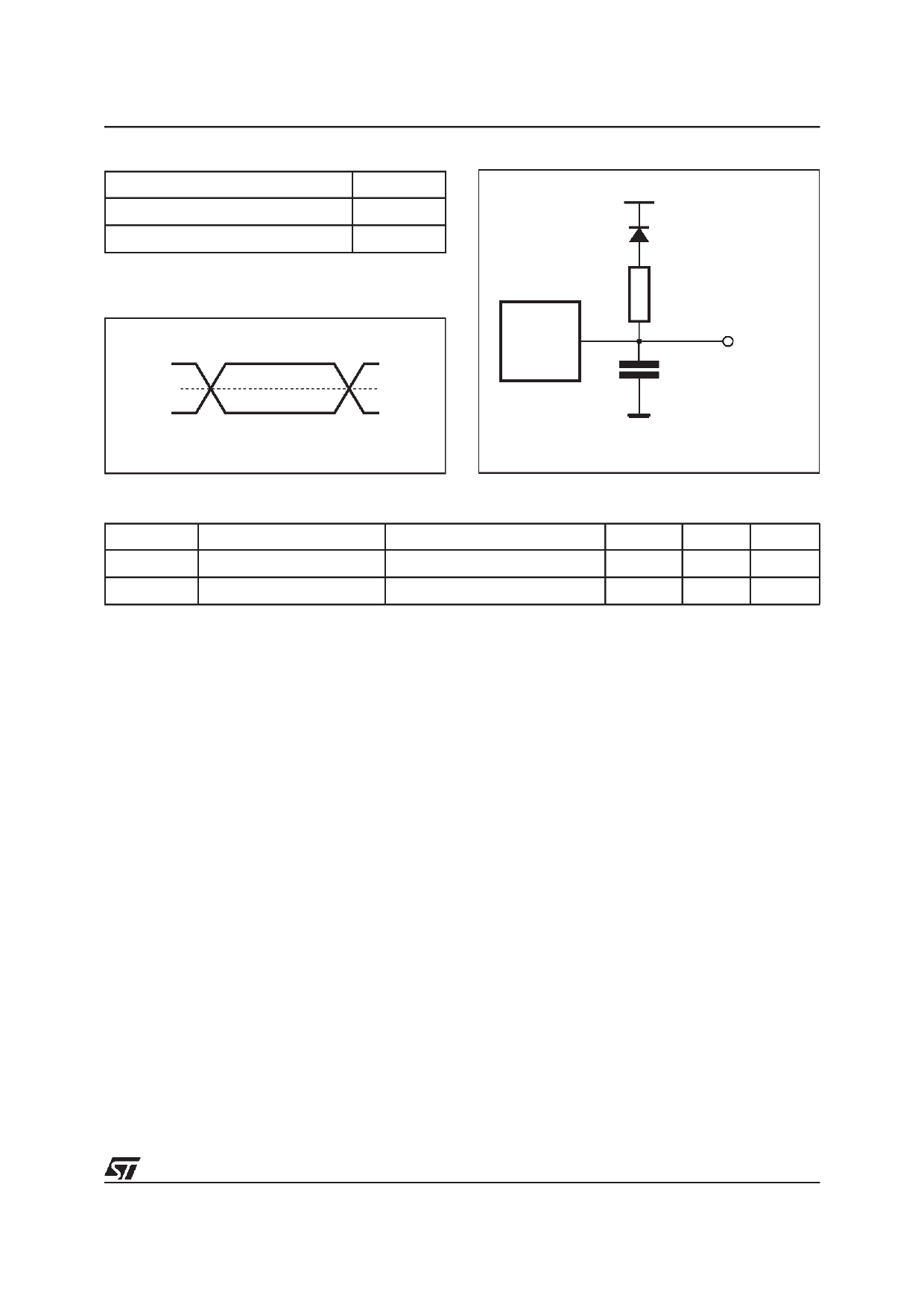
Table 21. AC Measurement Conditions
Input Rise and Fall Times
≤ 10ns
Input Pulse Voltages
0 to VDDQ
Input and Output Timing Ref. Voltages
VDDQ/2
Figure 5. AC Testing Input Output Waveform
VDDQ
0V
VDDQ/2
AI00610
M28W320CT, M28W320CB
Figure 6. AC Testing Load Circuit
VDDQ/2
1N914
DEVICE
UNDER
TEST
3.3kΩ
OUT
CL = 50pF
CL includes JIG capacitance
AI00609B
Table 22. Capacitance (1) (TA = 25 °C, f = 1 MHz)
Symbol
Parameter
Test Condition
CIN
Input Capacitance
VIN = 0V
COUT
Output Capacitance
VOUT = 0V
Note: 1. Sampled only, not 100% tested.
Min
Max
Unit
6
pF
12
pF
21/42
Share Link: 