SI4112G-BT 데이터 시트보기 (PDF) - Silicon Laboratories
부품명
상세내역
제조사
SI4112G-BT
Silicon Laboratories

SI4112G-BT Datasheet PDF : 32 Pages
| |||
Si4133G
Table 4. Serial Interface Timing
(VDD = 2.7 to 3.6 V, TA = –20 to 85°C)
Parameter1
Symbol
Test Condition
Min Typ Max Unit
SCLK Cycle Time
tclk
Figure 1
40
—
—
ns
SCLK Rise Time
tr
Figure 1
—
—
50
ns
SCLK Fall Time
tf
Figure 1
—
—
50
ns
SCLK High Time
th
Figure 1
10
—
—
ns
SCLK Low Time
tl
Figure 1
10
—
—
ns
SDATA Setup Time to SCLK↑2
tsu
Figure 2
5
—
—
ns
SDATA Hold Time from SCLK↑2
thold
Figure 2
0
—
—
ns
SENB↓ to SCLK↑ Delay Time2
ten1
Figure 2
10
—
—
ns
SCLK↑ to SENB↑ Delay Time2
ten2
Figure 2
12
—
—
ns
SENB↑ to SCLK↑ Delay Time2
ten3
Figure 2
12
—
—
ns
SENB Pulse Width
tw
Figure 2
10
—
—
ns
Notes:
1. All timing is referenced to the 50% level of the waveform, unless otherwise noted.
2. Timing is not referenced to 50% level of waveform. See Figure 2.
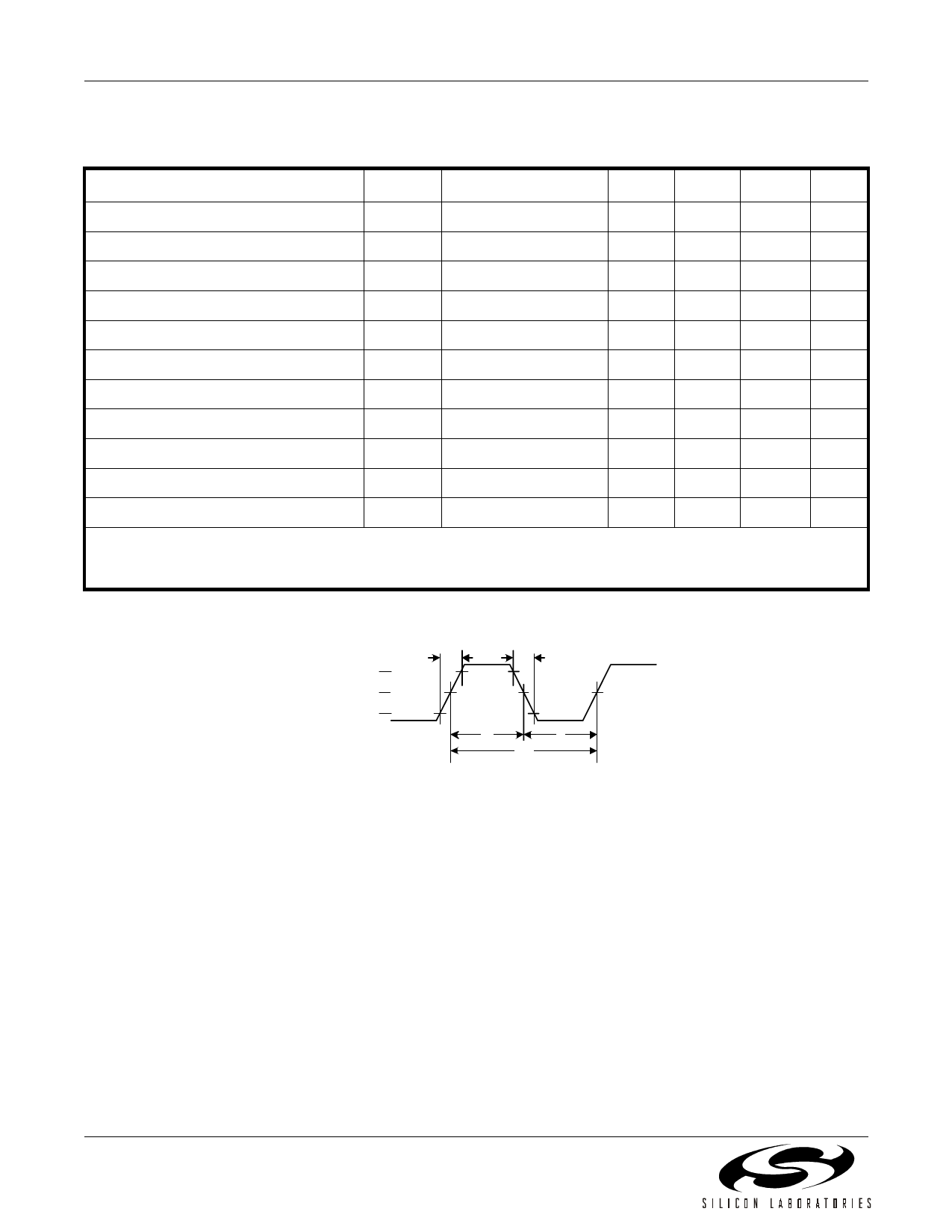
SCLK
80%
50%
20%
tr
tf
th
tl
t clk
Figure 1. SCLK Timing Diagram
6
Rev. 1.1
Share Link: