8183 데이터 시트보기 (PDF) - Allegro MicroSystems
부품명
상세내역
제조사
8183 Datasheet PDF : 8 Pages
| |||
8183
LOW-DROPOUT,
3 V REGULATOR
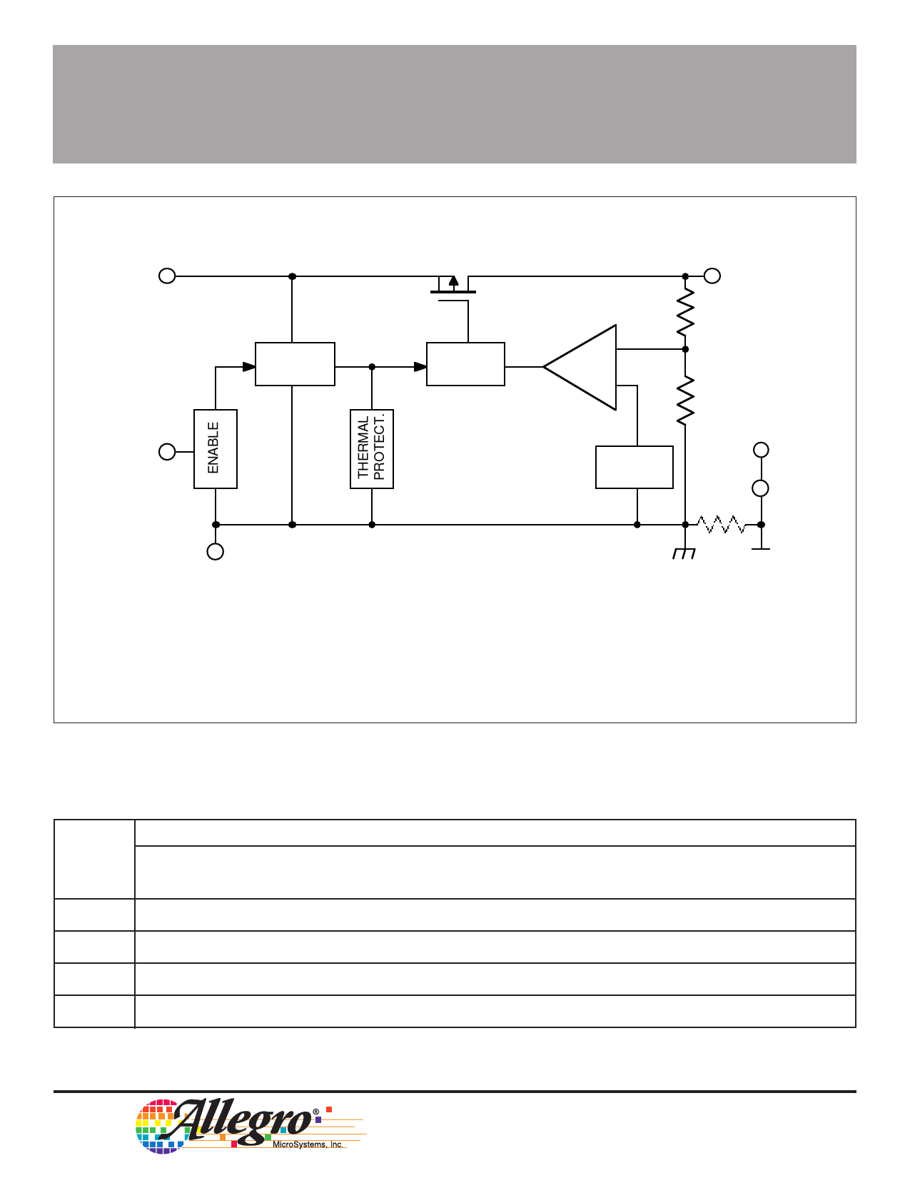
IN 4
FUNCTIONAL BLOCK DIAGRAM
6 OUT
ENABLE 3
BIAS
1 GND
DRIVE
ERROR
AMP
BANDGAP
REF.
2 SUB
5 SUB
SUB
Dwg. FS-012-3
Terminal numbering is in accordance with EIA/JEDEC convention.
Where EIAJ conventions apply, the tab is not numbered, resulting in
terminal 6 being designated terminal 5.
For proper operation, terminals 1 and 2 must be externally con-
nected together.
MAXIMUM ALLOWABLE OUTPUT CURRENT with device mounted on 2.24" x 2.24"
(56.9 mm x 56.9 mm) solder-coated copper-clad board in still air.
Maximum Allowable Output Current in Milliamperes with VI = 8 V, TJ = 150°C, Period ≤10 s*
dc (Duty Cycle)
TA
100%
90%
80%
70%
60%
50%
40%
30%
20%
25°C
95
105
120
135
150
150
150
150
150
50°C
75
85
95
110
125
150
150
150
150
70°C
60
65
75
85
100
120
150
150
150
85°C
50
55
60
70
80
100
125
150
150
* IO = (TJ - TA)/([VI - VO] RθJA • dc) = (150 - TA)/(5 • 258 • dc)
Output current rating can be increased (to 150 mA maximum) by heat sinking or reducing the input voltage. Conditions that produce excessive
junction temperature will activate device thermal shutdown circuitry. These conditions can be tolerated but should be avoided.
115 Northeast Cutoff, Box 15036
Worcester, Massachusetts 01615-0036 (508) 853-5000
Copyright © 1994 Allegro MicroSystems, Inc.
Share Link: 