MM1292KF 데이터 시트보기 (PDF) - Mitsumi
부품명
상세내역
제조사
MM1292KF Datasheet PDF : 7 Pages
| |||
MITSUMI
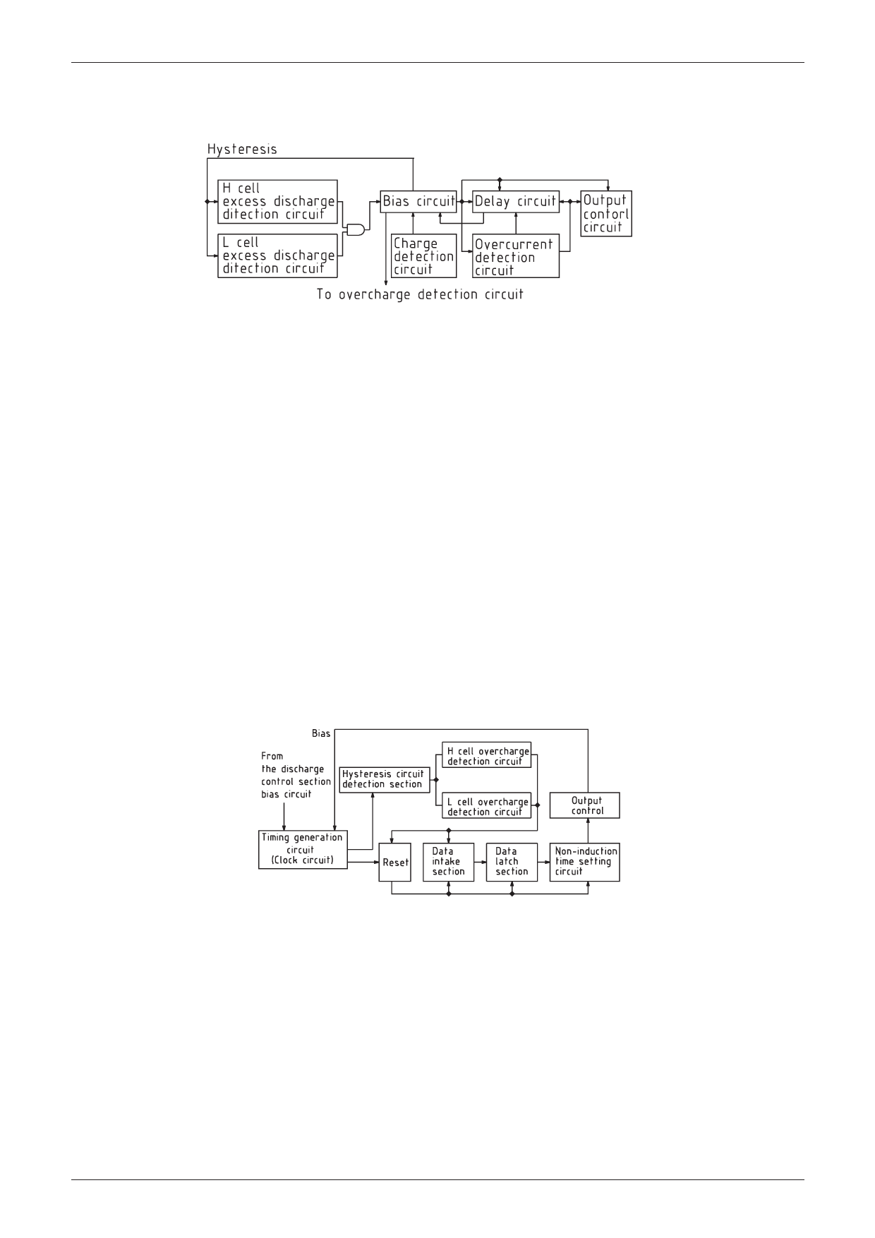
[Operation]
1. Excess discharge detection circuit
Protection of Lithium Ion Batteries (two cells in series) MM1292
The H cell excess discharge detection circuit monitors the voltage between VH-VL, while the L cell excess
discharge detection circuit monitors the voltage between VL-GND. When the voltage between VH-VL and VL-
GND exceeds VS, the operating state is maintained with bias current supplied from the bias circuit to the
delay circuit, the output control circuit, the overcurrent detection circuit, and the overcharge detection circuit.
When the battery current for either the H or L cell falls below VS, the current from the excess discharge
detection circuit to the bias circuit is switched off. Also, the capacitor connected to the delay circuit's
comparator (COD) input pin is charged using constant current. When this falls below the COD's reference
input potential, the bias current to output control and current to the bias circuit are switched off.
The excess discharge delay time (tOD) is set by the delay circuit and cannot be modified externally. When the
bias circuit is in waiting mode, the hysteresis loop to the excess discharge detection circuit is switched off,
and the detection voltage of the excess discharge detection circuit becomes discharge resumption voltage
(VDCH). When the battery is being charged and the voltage between CS-GND during excess discharge mode
falls below VST, however, start-up current is supplied to the bias circuit, and the hysteresis loop of the excess
discharge detection circuit is connected. Therefore, the excess discharge detection circuit detection voltage
becomes VS. Also, the overcharging detection circuit goes into waiting mode, so overcharging detection does
not occur in overcharging mode.
When the cell voltage of either the H or L cell exceeds VALM (one is excess discharging and the other is
overcharging), the bias current is maintained in the overcharging detection circuit. Therefore, the overcharging
is maintained until the current falls below VALM.
2. Overcharging Detection Circuit
The timing (clock) for the waiting interval and operating interval is created by the timing generation circuit. In
normal mode, the only blocks operating during the waiting interval are the input stages for the timing
generation circuit and the data intake section. Other blocks operate only during the operation interval.
The operation interval and the waiting interval are set at a ratio of 1:10, reducing power consumption. The
voltage detection resistance of the overcharge detection circuit is switched on and off by the detection
section's SW circuit. Therefore, current does not flow to detection resistors during waiting time, resulting in
low current consumption during excess discharge mode.
(Operating sequence)
Bias current is supplied to the timing generation circuit and data intake section by the bias circuit of the
excess discharge detection section during normal mode.
The operation interval and the waiting interval are created by the timing generation circuit. During the
operation interval, bias current is supplied to the excess charging detection circuit, and cell voltages of both
the H and L cells are monitored.
Share Link: 