74ACQ657SPC 데이터 시트보기 (PDF) - Fairchild Semiconductor
부품명
상세내역
제조사
74ACQ657SPC
Fairchild Semiconductor

74ACQ657SPC Datasheet PDF : 10 Pages
| |||
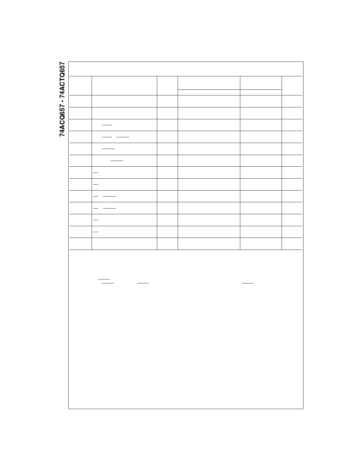
AC Electrical Characteristics for ACQ
VCC
TA = 25°C
TA = −40°C to +85°C
Symbol
Parameter
(V)
CL = 50 pF
CL = 50 pF
Units
(Note 13)
Min
Typ
Max
Min
Max
tPLH
Propagation Delay
tPHL
An to Bn, Bn to An
tPLH
Propagation Delay
tPHL
An to Parity
tPLH
Propagation Delay
tPHL
ODD/EVEN to PARITY
tPLH
Propagation Delay
tPHL
ODD/EVEN to ERROR
tPLH
Propagation Delay
tPHL
Bn to ERROR
tPLH
Propagation Delay
tPHL
PARITY to ERROR
tPZH
Output Enable Time
tPZL
OE to An/Bn
tPHZ
Output Disable Time
tPLZ
OE to An/Bn
tPZH
Output Enable Time
tPZL
OE to ERROR (Note 15)
tPHZ
Output Disable Time
tPLZ
OE to ERROR
tPZH
Output Enable Time
tPZL
OE to PARITY
tPHZ
Output Disable Time
tPLZ
OE to PARITY
tOSHL
Output to Output Skew (Note 14)
tOSLH
An, Bn to Bn, An
Note 13: Voltage Range 3.3 is 3.3V ± 0.3V
3.3
2.5
8.0
11.5
2.5
12.0
ns
5.0
1.5
5.0
7.5
1.5
8.0
3.3
3.0
11.5
16.5
3.0
17.0
ns
5.0
2.0
7.0
10.5
2.0
11.0
3.3
3.0
10.0
15.0
3.0
15.5
ns
5.0
2.5
6.5
10.0
2.5
10.5
3.3
3.0
10.0
15.0
3.0
15.5
ns
5.0
2.5
6.5
10.0
2.5
10.5
3.3
3.5
11.5
16.0
3.5
16.5
ns
5.0
2.5
7.0
10.5
2.5
11.0
3.3
3.0
9.0
13.5
3.0
14.0
ns
5.0
2.0
6.0
9.0
2.0
9.5
3.3
2.5
9.0
13.5
2.5
14.0
ns
5.0
2.0
6.0
9.0
2.0
9.5
3.3
1.0
8.5
13.0
1.0
13.5
ns
5.0
1.0
5.5
8.5
1.0
9.0
3.3
2.5
9.0
13.5
2.5
14.0
ns
5.0
2.0
6.0
9.0
2.0
9.5
3.3
1.0
8.5
13.0
1.0
13.5
ns
5.0
1.0
5.5
8.5
1.0
9.0
3.3
2.5
9.0
13.5
2.5
14.0
ns
5.0
2.0
6.0
9.0
2.0
9.5
3.3
1.0
8.5
13.0
1.0
13.5
ns
5.0
1.0
5.5
8.5
1.0
9.0
3.3
1.0
1.5
1.5
ns
5.0
0.5
1.0
1.0
Voltage Range 5.0 is 5.0V ± 0.5V
Note 14: Skew is defined as the absolute value of the difference between the actual propagation delay for any two outputs within the same packaged device.
The specification applies to any outputs switching in the same direction, either HIGH-to-LOW (tOSHL) or LOW-to-HIGH (tOSLH). Parameter guaranteed by
design. Not tested.
Note 15: These delay times reflect the 3-STATE recovery time only and not the signal time through the buffers or the parity check circuitry. To assure VALID
information at the ERROR pin, time must be allowed for the signal to propagate through the drivers (B to A), through the parity check circuitry (same as A to
PARITY), and to the ERROR output after the ERROR pin has been enabled (Output Enable times). VALID data at the ERROR pin ≥ (A to PARITY) +(Output
Enable Time).
www.fairchildsemi.com
6
Share Link: