HMS81C4316 데이터 시트보기 (PDF) - Hynix Semiconductor
부품명
상세내역
제조사
HMS81C4316 Datasheet PDF : 100 Pages
| |||
HMS81C43xx / GMS87C4060
8.2 Program Memory
A 16-bit program counter is capable of addressing up to
64K bytes, but HMS81C43xx/GMS87C4060 has 8~32K/
60K bytes program memory space only physically imple-
mented. Accessing a location above FFFFH will cause a
wrap-around to 0000H.
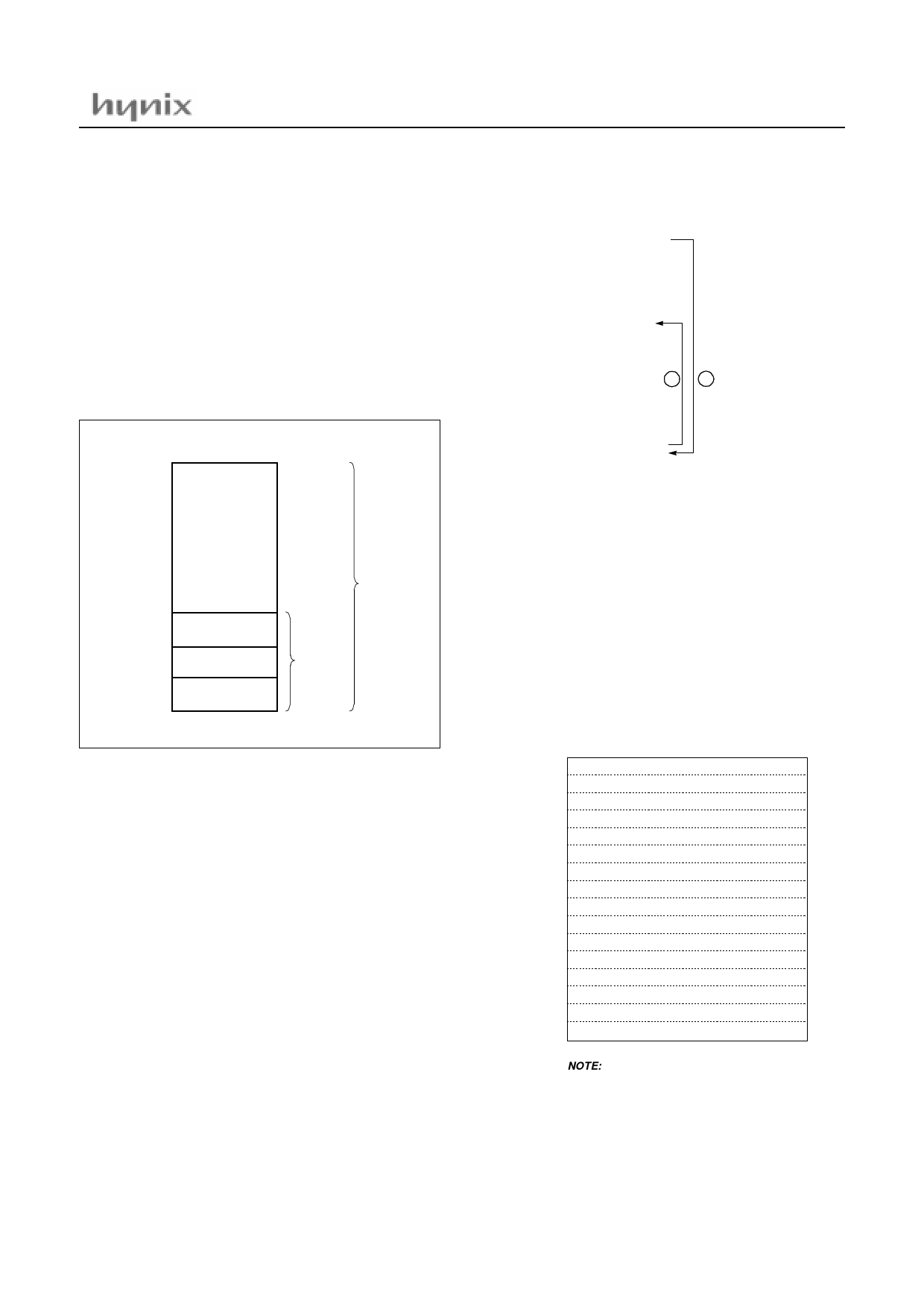
Figure 8-5 , shows a map of Program Memory. After reset,
the CPU begins execution from reset vector which is stored
in address FFFEH and FFFFH as shown in Figure 8-6 .
As shown in Figure 8-5 , each area is assigned a fixed lo-
cation in Program Memory. Program Memory area con-
tains the user program.
87C4060:1000H
81C4332:8000H
81C4324:A000H
81C4316:C000H
81C4308:E000H
FEFFH
FF00H
FFBFH
FFC0H
FFDFH
FFE0H
FFFFH
TCALL
AREA
INTERRUPT
VECTOR AREA
PROGRAM
MEMORY
PCALL
AREA
Figure 8-5 Program Memory Map
Page Call (PCALL) area contains subroutine program to
reduce program byte length by using 2 bytes PCALL in-
stead of 3 bytes CALL instruction. If it is frequently called,
it is more useful to save program byte length.
Table Call (TCALL) causes the CPU to jump to each
TCALL address, where it commences the execution of the
service routine. The Table Call service area spaces 2-byte
for every TCALL: 0FFC0H for TCALL15, 0FFC2H for
TCALL14, etc., as shown in Figure 8-7 .
Example: Usage of TCALL
LDA #5
TCALL 0FH
:
:
;
;TABLE CALL ROUTINE
;
FUNC_A: LDA LRG0
RET
;
FUNC_B: LDA LRG1 2
RET
;
;TABLE CALL ADD. AREA
;
ORG 0FFC0H
DW FUNC_A
DW FUNC_B
;1B Y TE INS T RU CT IO N
;IN S TE A D O F 2 B Y TE S
;N O R M A L CA LL
1
;TC A LL A DD R E SS A RE A
The interrupt causes the CPU to jump to specific location,
where it commences the execution of the service routine.
The External interrupt 0, for example, is assigned to loca-
tion 0FFFCH. The interrupt service locations spaces 2-byte
interval: 0FFF8H and 0FFF9H for External Interrupt 1,
0FFFCH and 0FFFDH for External Interrupt 0, etc.
Any area from 0FF00H to 0FFFFH, if it is not going to be
used, its service location is available as general purpose
Program Memory.
Address
0FFE0H
E2
E4
E6
E8
EA
EC
EE
F0
F2
F4
F6
F8
FA
FC
FE
Vector Area Memory
I2C Bus Interface Interrupt Vector Area
Serial I/O Interrupt Vector Area
Basic Interval Timer Interrupt Vector Area
Watchdog Timer Interrupt Vector Area
External Interrupt 3/4 Vector Area
Timer/Counter 3 Interrupt Vector Area
Timer/Counter 1 Interrupt Vector Area
V-Sync Interrupt Vector Area
1 Frame Timer Interrupt Vector Area
Timer/Counter 2 Interrupt Vector Area
Timer/Counter 0 Interrupt Vector Area
External Interrupt 2 Vector Area
External Interrupt 1 Vector Area
On Screen Display Interrupt Vector Area
External Interrupt 0 Vector Area
RESET Vector Area
NOTE:
"-" means reserved area.
Figure 8-6 Interrupt Vector Area
November 2001 ver 1.2
21
Share Link: 