EL2060CS 데이터 시트보기 (PDF) - Elantec -> Intersil
부품명
상세내역
제조사
EL2060CS Datasheet PDF : 16 Pages
| |||
EL2160C
130 MHz Current Feedback Amplifier
Applications Information Contd
Supply Voltage Range
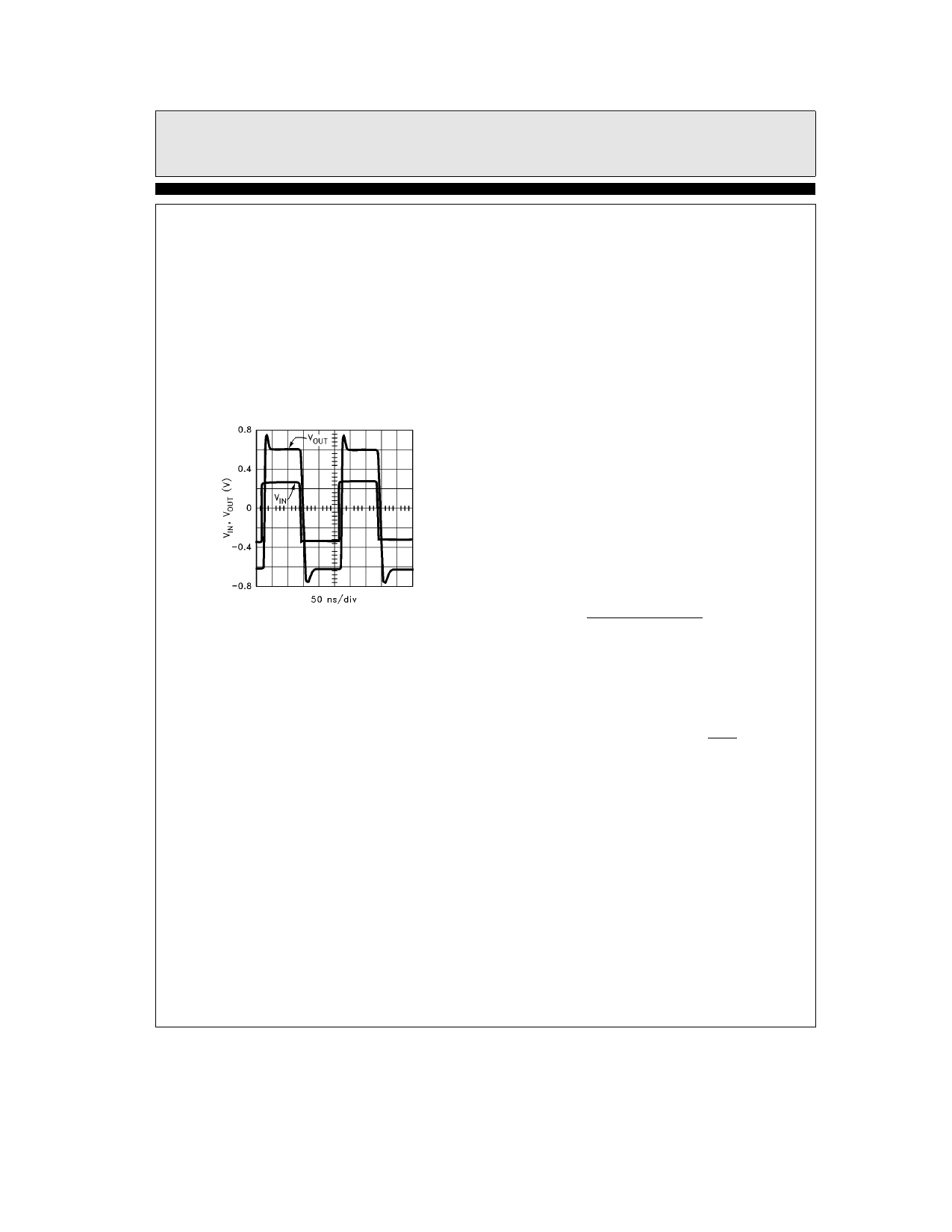
The EL2160C has been designed to operate with
supply voltages from g2V to g15V Optimum
bandwidth slew rate and video characteristics
are obtained at higher supply voltages However
at g2V supplies the 3 dB bandwidth at AV e
a2 is a respectable 70 MHz The following figure
is an oscilloscope plot of the EL2160C at g2V
supplies AV e a2 RF e RG e 560X driving a
load of 150X showing a clean g600 mV signal at
the output
2060 – 11
If a single supply is desired values from a4V to
a30V can be used as long as the input common
mode range is not exceeded When using a single
supply be sure to either 1) DC bias the inputs at
an appropriate common mode voltage and AC
couple the signal or 2) ensure the driving signal
is within the common mode range of the
EL2160C
Settling Characteristics
The EL2160C offers superb settling characteris-
tics to 0 1% typically in the 35 ns to 40 ns range
There are no aberrations created from the input
stage which often cause longer settling times in
other current feedback amplifiers The EL2160C
is not slew rate limited therefore any size step up
to g10V gives approximately the same settling
time
As can be seen from the Long Term Settling Er-
ror curve for AV e a1 there is approximately a
0 035% residual which tails away to 0 01% in
about 40 ms This is a thermal settling error
caused by a power dissipation differential (before
and after the voltage step) For AV e b1 due to
the inverting mode configuration this tail does
not appear since the input stage does not experi-
ence the large voltage change as in the non-
inverting mode With AV e b1 0 01% settling
time is slightly greater than 100 ns
Power Dissipation
The EL2160C amplifier combines both high
speed and large output current drive capability at
a moderate supply current in very small pack-
ages It is possible to exceed the maximum junc-
tion temperature allowed under certain supply
voltage temperature and loading conditions To
ensure that the EL2160C remains within its abso-
lute maximum ratings the following discussion
will help to avoid exceeding the maximum junc-
tion temperature
The maximum power dissipation allowed in a
package is determined by its thermal resistance
and the amount of temperature rise according to
PDMAX
e
TJMAX b TAMAX
iJA
The maximum power dissipation actually pro-
duced by an IC is the total quiescent supply cur-
rent times the total power supply voltage plus
the power in the IC due to the load or
PDMAX e 2
VS
IS a (VS b VOUT)
VOUT
RL
where IS is the supply current (To be more accu-
rate the quiescent supply current flowing in the
output driver transistor should be subtracted
from the first term because under loading and
due to the class AB nature of the output stage
the output driver current is now included in the
second term )
In general an amplifier’s AC performance de-
grades at higher operating temperature and lower
supply current Unlike some amplifiers the
EL2160C maintains almost constant supply
13
Share Link: 