ADCMP604(Rev0) 데이터 시트보기 (PDF) - Analog Devices
부품명
상세내역
제조사
ADCMP604
(Rev.:Rev0)
(Rev.:Rev0)
ADCMP604 Datasheet PDF : 16 Pages
| |||

ADCMP604/ADCMP605
250
200
150
100
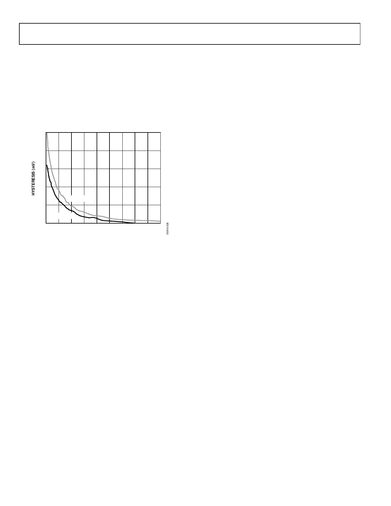
VCC = 2.5V
50
VCC = 5.5V
0
50 100 150 200 250 300 350 400 450 500
HYSTERESIS RESISTOR (kΩ)
Figure 20. Hysteresis vs. RHYS Control Resistor
CROSSOVER BIAS POINTS
Rail-to-rail inputs of this type, in both op amps and
comparators, have a dual front-end design. Certain devices are
active near the VCC rail and others are active near the VEE rail. At
some predetermined point in the common-mode range, a
crossover occurs. At this point, normally VCC/2, the direction of
the bias current reverses and there are changes in measured offset
voltages and currents.
MINIMUM INPUT SLEW RATE REQUIREMENT
With the rated load capacitance and normal good PC Board
design practice, as discussed in the Optimizing Performance
section, these comparators should be stable at any input slew
rate with no hysteresis. Broadband noise from the input stage is
observed in place of the violent chattering seen with most other
high speed comparators. With additional capacitive loading or
poor bypassing, oscillation is observed. This oscillation is due to
the high gain bandwidth of the comparator in combination with
feedback parasitics in the package and PC board. In many
applications, chattering is not harmful.
Rev. 0 | Page 12 of 16