AT49BV1604 데이터 시트보기 (PDF) - Atmel Corporation
부품명
상세내역
제조사
AT49BV1604 Datasheet PDF : 18 Pages
| |||
AT49BV1604(T)/1614(T)
A VPP pin is provided to improve program/erase times. This
pin can be tied to VCC. To take advantage of faster pro-
gramming and erasing, the pin should supply 4.5 to 5.5
volts during program and erase operations.
A six byte command (bypass unlock) sequence to remove
the requirement of entering the three byte program
sequence is offered to further improve programming time.
After entering the six byte code, only single pulses on the
write control lines are required for writing into the device.
This mode (single pulse byte/word program) is exited by
powering down the device, or by pulsing the RESET pin
low for a minimum of 50 ns and then bringing it back to VCC.
Erase and Erase Suspend/Resume commands will not
work while in this mode; if entered they will result in data
being programmed into the device. It is not recommended
that the six byte code reside in the software of the final
product but only exist in external programming code.
For the AT49BV1614(T), the BYTE pin controls whether
the device data I/O pins operate in the byte or word config-
uration. If the BYTE pin is set at logic “1”, the device is in
word configuration, I/O0-I/O15 are active and controlled by
CE and OE.
If the BYTE pin is set at logic “0”, the device is in byte con-
figuration, and only data I/O pins I/O0 - I/O7 are active and
controlled by CE and OE. The data I/O pins I/O8 - I/O14
are tri-stated, and the I/O15 pin is used as an input for the
LSB (A-1) address function.
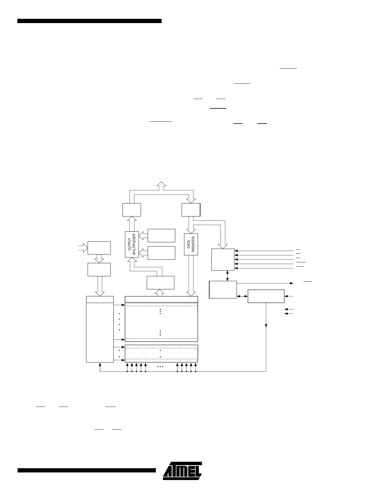
Block Diagram
I/O0 - I/O15/A-1
OUTPUT
BUFFER
INPUT
BUFFER
A0 - A19
INPUT
BUFFER
ADDRESS
LATCH
Y-DECODER
X-DECODER
IDENTIFIER
REGISTER
STATUS
REGISTER
DATA
COMPARATOR
Y-GATING
PLANE B
SECTORS
COMMAND
REGISTER
WRITE STATE
MACHINE
PROGRAM/ERASE
VOLTAGE SWITCH
CE
WE
OE
RESET
BYTE
RDY/BUSY
VPP
VCC
GND
PLANE A SECTORS
Device Operation
READ: The AT49BV16X4(T) is accessed like an EPROM.
When CE and OE are low and WE is high, the data stored
at the memory location determined by the address pins are
asserted on the outputs. The outputs are put in the high
impedance state whenever CE or OE is high. This dual-line
control gives designers flexibility in preventing bus
contention.
COMMAND SEQUENCES: When the device is first pow-
ered on it will be reset to the read or standby mode
depending upon the state of the control line inputs. In order
to perform other device functions, a series of command
sequences are entered into the device. The command
sequences are shown in the Command Definitions table
(I/O8 - I/O15 are don't care inputs for the command codes).
3
Share Link: 