CC2430ZDK 데이터 시트보기 (PDF) - TEXAS ADVANCED OPTOELECTRONIC SOLUTIONS
부품명
상세내역
제조사
CC2430ZDK
TEXAS ADVANCED OPTOELECTRONIC SOLUTIONS

CC2430ZDK Datasheet PDF : 212 Pages
| |||
CC2430
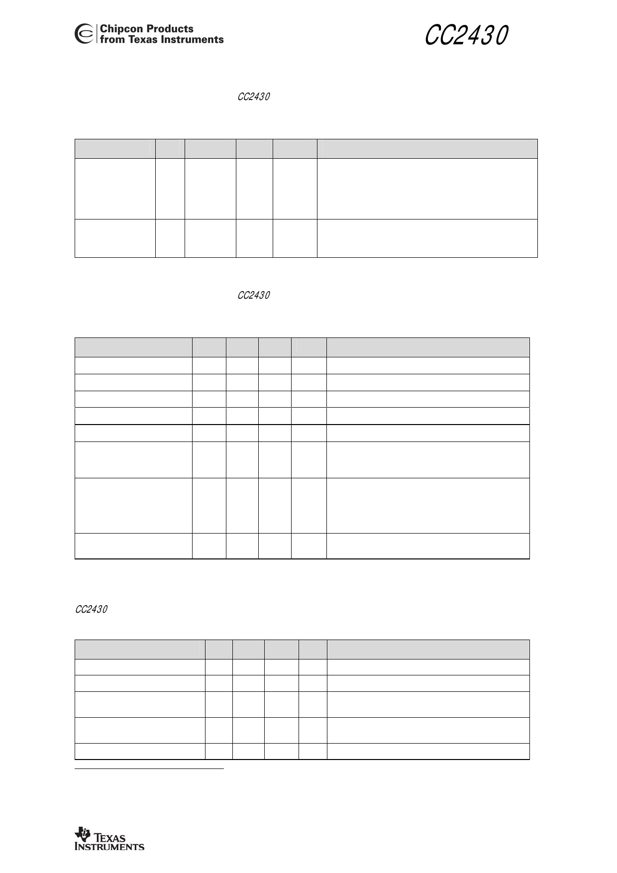
7.8 Frequency Synthesizer Characteristics
Measured on Texas Instruments CC2430 EM reference design with TA=25°C and VDD=3.0V
unless stated otherwise.
Table 12: Frequency Synthesizer Parameters
Parameter
Min
Typ
Max Unit
Condition/Note
Phase noise
−116
−117
−118
dBc/Hz
dBc/Hz
dBc/Hz
Unmodulated carrier
At ±1.5 MHz offset from carrier
At ±3 MHz offset from carrier
At ±5 MHz offset from carrier
PLL lock time
192 µs
The startup time until RX/TX turnaround. The crystal
oscillator is running.
7.9 Analog Temperature Sensor
Measured on Texas Instruments CC2430 EM reference design with TA=25°C and VDD=3.0V
unless stated otherwise.
Table 13: Analog Temperature Sensor Parameters
Parameter
Min Typ Max Unit Condition/Note
Output voltage at –40°C
Output voltage at 0°C
Output voltage at +40°C
Output voltage at +80°C
Temperature coefficient
Absolute error in calculated
temperature
Error in calculated
temperature, calibrated
Current consumption
increase when enabled
0.648
V
Value is estimated
0.743
V
Value is estimated
0.840
V
Value is estimated
0.939
V
Value is estimated
2.45
mV/°C Fitted from –20°C to +80°C on estimated values.
–8
°C
From –20°C to +80°C when assuming best fit for
absolute accuracy on estimated values: 0.743V at
0°C and 2.45mV / °C.
-2
0
2 °C
From –20°C to +80°C when using 2.45mV / °C,
after 1-point calibration at room temperature.
Values are estimated. Indicated min/max with 1-
point calibration is based on simulated values for
typical process parameters
280
µA
7.10 ADC
Measured with TA=25°C and VDD=3.0V. Note that other data may result using Texas Instruments
CC2430 EM reference design.
Table 14: ADC Characteristics
Parameter
Min Typ Max Unit Condition/Note
Input voltage
External reference voltage
External reference voltage
differential
Input resistance, signal
Full-Scale Signal3
0
VDD V
VDD is voltage on AVDD_SOC pin
0
VDD V
VDD is voltage on AVDD_SOC pin
0
VDD V
VDD is voltage on AVDD_SOC pin
197
kΩ Simulated using 4 MHz clock speed (see section
13.10.2.7)
2.97
V
Peak-to-peak, defines 0dBFS
3 Measured with 300 Hz Sine input and VDD as reference.
CC2430 Data Sheet (rev. 2.1) SWRS036F
Page 16 of 211
Share Link: