CC2430F32RTC 데이터 시트보기 (PDF) - TEXAS ADVANCED OPTOELECTRONIC SOLUTIONS
부품명
상세내역
제조사
CC2430F32RTC
TEXAS ADVANCED OPTOELECTRONIC SOLUTIONS

CC2430F32RTC Datasheet PDF : 212 Pages
| |||
CC2430
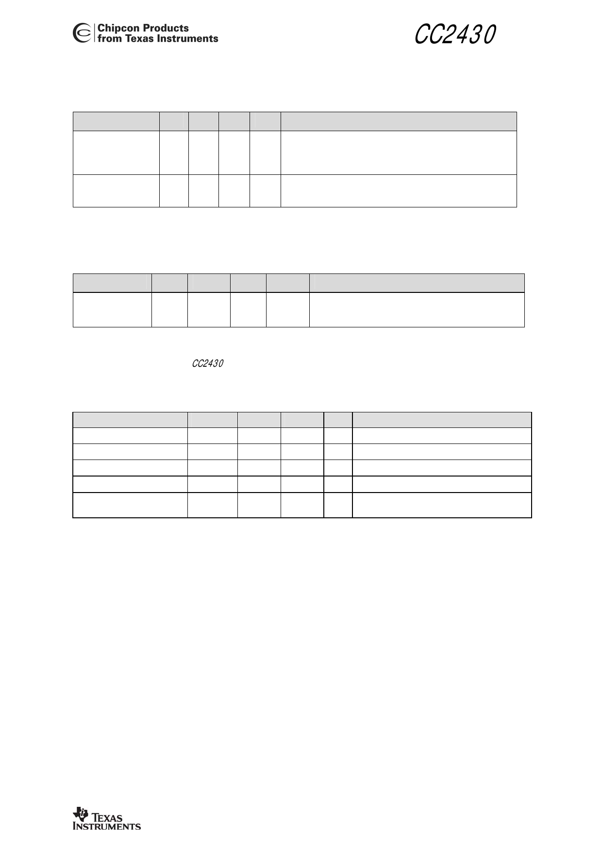
7.14 Port Outputs AC Characteristics
TA= 25°C, VDD=3.0V if nothing else stated.
Table 18: Port Outputs AC Characteristics
Parameter
P0_[0:7], P1_[2:7],
P2_[0:4] Port output
rise time
(SC=0/SC=1)
fall time
(SC=0/SC=1)
Min Typ Max Unit
3.15/
ns
1.34
3.2/
1.44
Condition/Note
Load = 10 pF
Timing is with respect to 10% VDD and 90% VDD levels.
Values are estimated
Load = 10 pF
Timing is with respect to 90% VDD and 10% VDD.
Values are estimated
7.15 Timer Inputs AC Characteristics
TA= -40°C to 85°C, VDD=2.0V to 3.6V if nothing else stated.
Table 19: Timer Inputs AC Characteristics
Parameter
Min
Typ
Max Unit
Condition/Note
Input capture
pulse width
tSYSCLK
ns
Synchronizers determine the shortest input pulse that
can be recognized. The synchronizers operate at the
current system clock rate (16 or 32 MHz)
7.16 DC Characteristics
The DC Characteristics of CC2430 are listed in Table 20 below.
TA=25°C, VDD=3.0V if nothing else stated.
Table 20: DC Characteristics
Digital Inputs/Outputs
Min
Typ
Logic "0" input voltage
Logic "1" input voltage
VDD-0.5
Logic "0" input current
NA
Logic "1" input current
NA
I/O pin pull-up and pull-down
20
resistor
Max Unit Condition
0.5
V
V
–1
µA Input equals 0V
1
µA Input equals VDD
kΩ
CC2430 Data Sheet (rev. 2.1) SWRS036F
Page 21 of 211
Share Link: