GT28F800F3T95 데이터 시트보기 (PDF) - Intel
부품명
상세내역
제조사
GT28F800F3T95 Datasheet PDF : 47 Pages
| |||
E
FAST BOOT BLOCK DATASHEET
4.1 Read Array Command
Upon initial device power-up or exit from reset, the
device defaults to read array mode. The read
configuration register defaults to asynchronous
page-mode. The Read Array command also causes
the device to enter read array mode. The device
remains enabled for reads until another command
is written. Once the internal WSM has started a
block erase or program, the device will not
recognize the Read Array command until the WSM
completes its operation or unless the WSM is
suspended via an Erase or Program Suspend
command. The Read Array command functions
independently of the VPP voltage.
4.2 Read Identifier Codes
Command
The identifier code operation is initiated by writing
the Read Identifier Codes command. After writing
the command, read cycles retrieve the
manufacturer and device codes (see Table 4 for
identifier code values). Page-mode and burst reads
are not supported in this read mode. To terminate
the operation, write another valid command, like the
Read Array command. The Read Identifier Codes
command functions independently of the VPP
voltage.
Table 4. Identifier Codes
Code
Address
(Hex)
Manufacturer Code
Device Code 8 Mbit -T
-B
16 Mbit -T
-B
00000
00001
00001
00001
00001
Data
(Hex)
0089
88F1
88F2
88F3
88F4
4.3 Read Status Register
Command
The status register can be read at any time by
writing the Read Status Register command to the
CUI. After writing this command, all subsequent
read operations output status register data until
another valid command is written. Page-mode and
burst reads are not supported in this read mode.
The status register content is updated and latched
on the rising edge of ADV# or rising (falling) CLK
edge when ADV# is low during synchronous burst-
mode or the falling edge of OE# or CE#, whichever
occurs first. The Read Status Register command
functions independently of the VPP voltage.
4.4 Clear Status Register
Command
Status register bits SR.5, SR.4, SR.3, and SR.1 are
set to “1”s by the WSM and can only be cleared by
issuing the Clear Status Register command. These
bits indicate various error conditions. By allowing
system software to reset these bits, several
operations may be performed (such as cumulatively
erasing or writing several bytes in sequence). The
status register may be polled to determine if a
problem occurred during the sequence. The Clear
Status Register command functions independently
of the applied VPP voltage. After executing this
command, the device returns to read array mode.
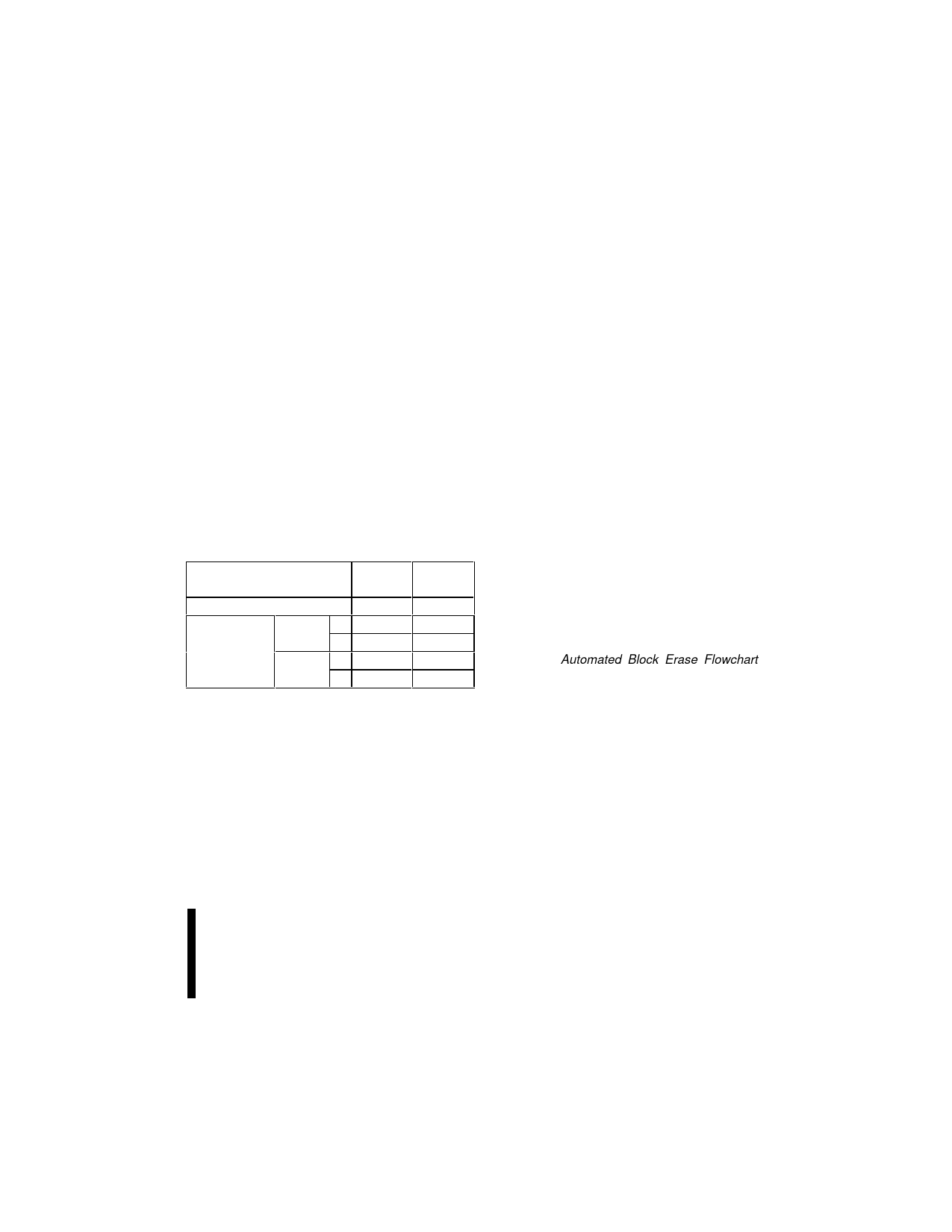
4.5 Block Erase Command
Erase is executed one block at a time and initiated
by a two-cycle command. A block erase setup is
written first, followed by a block erase confirm. This
command sequence requires appropriate
sequencing and address within the block to be
erased (erase changes all block data to FFH).
Block preconditioning, erase, and verify are handled
internally by the WSM. After the two-cycle block
erase sequence is written, the device automatically
outputs status register data when read (see
Figure 7, Automated Block Erase Flowchart). The
CPU can detect block erase completion by
analyzing status register bit SR.7.
When the block erase completes, check status
register bit SR.5 for an error flag (“1”). If an error is
detected, check status register bits SR.4, SR.3, and
SR.1 to understand what caused the failure. After
examining the status register, it should be cleared if
an error was detected before issuing a new
command. The device will remain in status register
read mode until another command is written to the
CUI.
PRODUCT PREVIEW
15
Share Link: 