MTSF3N03HDR2 데이터 시트보기 (PDF) - Motorola => Freescale
부품명
상세내역
제조사
MTSF3N03HDR2 Datasheet PDF : 12 Pages
| |||
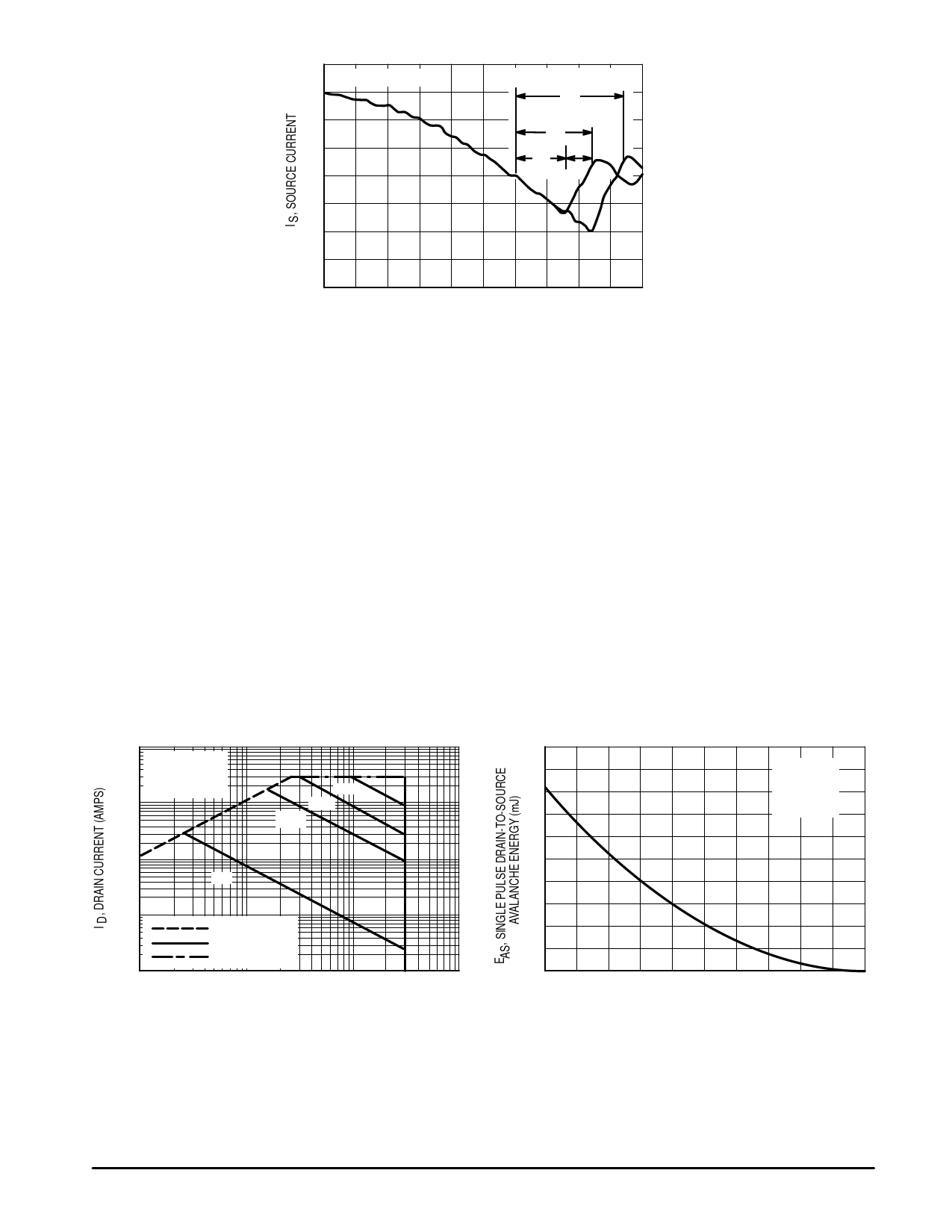
di/dt = 300 A/µs
Standard Cell Density
trr
High Cell Density
trr
ta
tb
MTSF3N03HD
t, TIME
Figure 13. Reverse Recovery Time (trr)
SAFE OPERATING AREA
The Forward Biased Safe Operating Area curve (Figure
14) defines the maximum simultaneous drain–to–source vol-
tage and drain current that a transistor can handle safely
when it is forward biased. Curves are based upon maximum
peak junction temperature and a case temperature (TC) of
25°C. Peak repetitive pulsed power limits are determined by
using the thermal response data in conjunction with the pro-
cedures discussed in AN569, “Transient Thermal Resistance
– General Data and Its Use.”
Switching between the off–state and the on–state may tra-
verse any load line provided neither rated peak current (IDM)
nor rated voltage (VDSS) is exceeded, and that the transition
time (tr, tf) does not exceed 10 µs. In addition the total power
averaged over a complete switching cycle must not exceed
(TJ(MAX) – TC)/(RθJC).
A power MOSFET designated E–FET can be safely used
in switching circuits with unclamped inductive loads. For reli-
able operation, the stored energy from circuit inductance dis-
sipated in the transistor while in avalanche must be less than
the rated limit and must be adjusted for operating conditions
differing from those specified. Although industry practice is to
rate in terms of energy, avalanche energy capability is not a
constant. The energy rating decreases non–linearly with an
increase of peak current in avalanche and peak junction tem-
perature.
Although many E–FETs can withstand the stress of drain–
to–source avalanche at currents up to rated pulsed current
(IDM), the energy rating is specified at rated continuous cur-
rent (ID), in accordance with industry custom. The energy rat-
ing must be derated for temperature as shown in the
accompanying graph (Figure 15). Maximum energy at cur-
rents below rated continuous ID can safely be assumed to
equal the values indicated.
100
VGS = 20 V
SINGLE PULSE
TC = 25°C
10
100 µs
1 ms
10 ms
1
dc
0.1
0.01
0.1
RDS(on) LIMIT
THERMAL LIMIT
PACKAGE LIMIT
1
10
100
VDS, DRAIN–TO–SOURCE VOLTAGE (VOLTS)
Figure 14. Maximum Rated Forward Biased
Safe Operating Area
250
VDD = 30 V
200
VGS = 5 V
IL = 9 A
L = 5 mH
150
100
50
0
25
50
75
100
125
150
TJ, STARTING JUNCTION TEMPERATURE (°C)
Figure 15. Maximum Avalanche Energy versus
Starting Junction Temperature
Motorola TMOS Power MOSFET Transistor Device Data
7
Share Link: 