M80C186EB 데이터 시트보기 (PDF) - Intel
부품명
상세내역
제조사
M80C186EB Datasheet PDF : 56 Pages
| |||
M80C186EB
PACKAGE INFORMATION
This section describes the pins pinouts and thermal
characteristics for the M80C186EB PGA package
For complete package specifications and informa-
tion see the Intel Packaging Outlines and Dimen-
sions Guide (Order Number 231369)
Pin Descriptions
The M80C186EB pins are described in this section
Table 3 presents the legend for interpreting the pin
descriptions in Table 4 Figure 7 provides an exam-
ple pin description entry The ‘‘I O’’ signifies that the
pins are bidirectional (i e have both an input and
output function) The ‘‘S’’ indicates that as an input
the signal is synchronized to CLKOUT for proper op-
eration The ‘‘H(Z)’’ indicates that these pins will
float while the processor is in the Hold Acknowledge
state R(Z) indicates that these pins will float while
RESIN is low P(X) Indicates that these pins will re-
tain its current value when Idle or Powerdown
Modes are entered
All pins float while the processor is in the ONCE
Mode except OSCOUT (OSCOUT is required for
crystal operation)
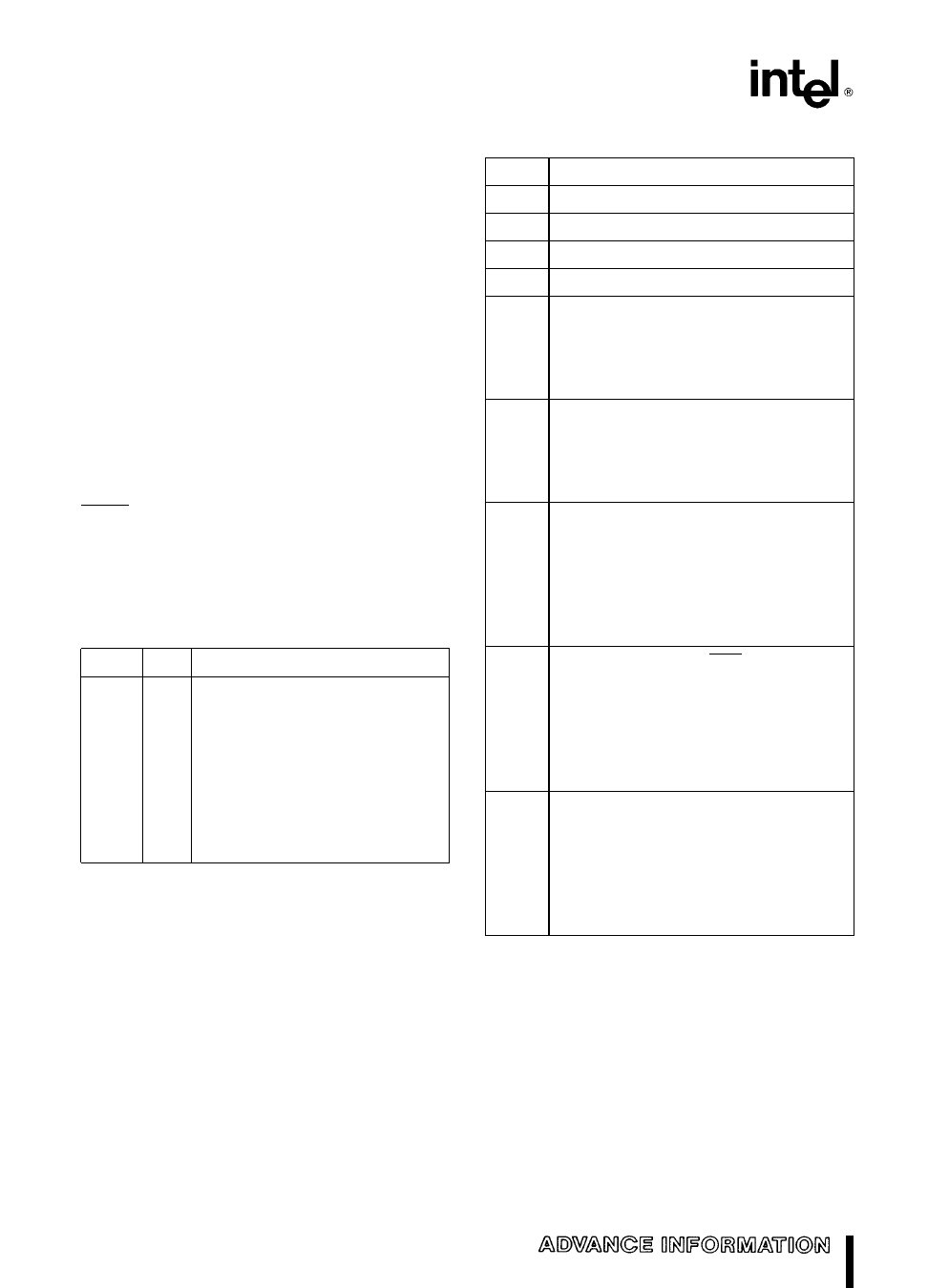
Name Type
Description
AD15 0
IO
S(L)
H(Z)
R(Z)
P(X)
These pins provide a multiplexed
ADDRESS and DATA bus During
the address phase of the bus
cycle address bits 0 through 15
are presented on the bus and can
be latched using ALE 8- or 16-bit
data information are transferred
during the data phase of the bus
cycle
Figure 7 Example Pin Description Entry
Table 3 Pin Description Nomenclature
Symbol
Description
I Input Only Pin
O Output Only Pin
I O Pin can be either input or output
Pin ‘‘must be’’ connected as described
S( ) Synchronous Input must meet setup and
hold times for proper operation of the
processor The pin is
S(E) edge sensitive
S(L) level sensitive
A( ) Asynchronous Input must meet setup and
hold only to guarantee recognition The
pin is
A(E) edge sensitive
A(L) level sensitive
H( ) While the processor’s bus is in the Hold
Acknowledge state the pin
H(1) is driven to VCC
H(0) is driven to VSS
H(Z) floats
H(Q) remains active
H(X) retains current state
R( ) While the processor’s RES line is low the
pin
R(1) is driven to VCC
R(0) is driven to VSS
R(Z) floats
R(WH) weak pullup
R(WL) weak pulldown
P( ) While Idle or Powerdown modes are
active the pin
P(1) is driven to VCC
P(0) is driven to VSS
P(Z) floats
P(Q) remains active(1)
P(X) retains current state
NOTE
1 Any pin that specifies P(Q) are valid for Idle
Mode All pins are P(X) for Powerdown Mode
14
Share Link: 