NT7701H-BDT 데이터 시트보기 (PDF) - Novatek Microelectronics
부품명
상세내역
제조사
NT7701H-BDT Datasheet PDF : 37 Pages
| |||
NT7701
Absolute Maximum Rating*
DC Supply Voltage VDD . . . . . . . . . . . . -0.3V to +7.0V
DC Supply Voltage V0 . . . . . . . . . . . . . -0.3V to +30V
Input Voltage . . . . . . . . . . . . . . . . . -0.3V to VDD +0.3V
Operating Ambient Temperature . . . . -30°C to +85°C
Storage Temperature . . . . . . . . . . . . .-45°C to +125°C
*Comments
Stresses above those listed under "Absolute Maximum
Ratings" may cause permanent damage to this device.
These are stress ratings only. Functional operation of this
device under these or any other conditions above those
indicated in the operational sections of this specification is
not implied or intended. Exposure to the absolute maximum
rating conditions for extended periods may affect device
reliability.
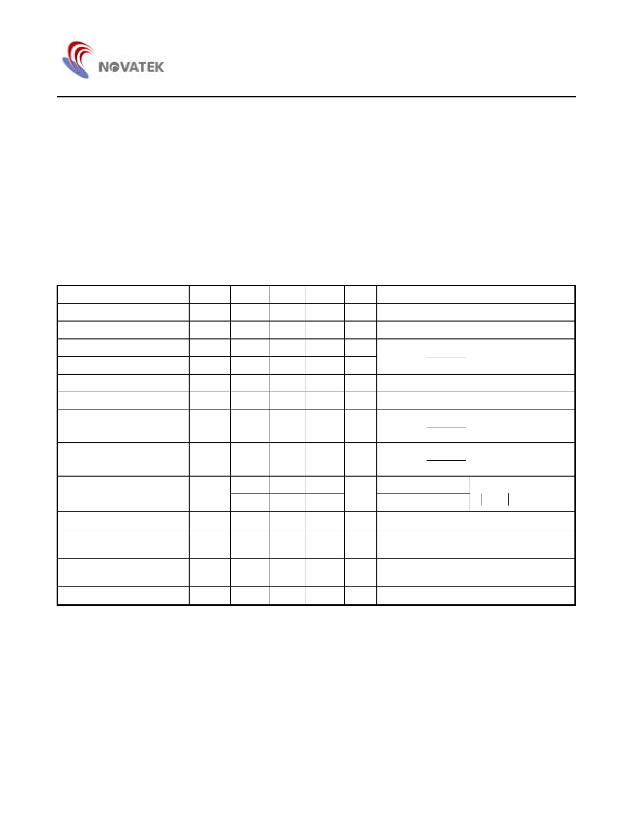
Electrical Characteristics
DC Characteristics
Segment Mode (VSS = V5 = 0V, VDD = 2.5 - 5.5V, V0 = 15 to 30 V, and TA = -30 to +85°C, unless otherwise noted)
Parameter
Symbol Min. Typ. Max. Unit
Condition
Operating Voltage
VDD
2.5
-
5.5
V
Operating Voltage
V0
15
-
30
V
Input high voltage
Input low voltage
VIH 0.8 VDD -
-
V D0 - 7, XCK, LP, L/R, FR, MD, S/C, EIO1,
VIL
-
- 0.2 VDD V EIO2 and DISPOFF pins
Output high voltage
VOH VDD - 0.4 -
-
V EIO1, EIO2 pins, IOH = -0.4mA
Output low voltage
VOL
-
-
+0.4
V EIO1, EIO2 pins, IOL = +0.4mA
Input leakage current 1
D0 - 7, XCK, LP, L/R, FR, MD, S/C, EIO1,
IIH
-
-
+1
µA EIO2 and DISPOFF pins, VI = VDD
Input leakage current 2
D0 - 7, XCK, LP, L/R, FR, MD, S/C, EIO1,
IIL
-
-
-1
µA EIO2 and DISPOFF pins, VI = VSS
Output resistance
-
1.0
1.5
V0 = +30.0V
RON
kΩ
-
1.5
2.0
V0 = +20.0V
Y1 - Y160 pins,
∆V O N = 0.5V
Stand-by current
ISB
-
-
5
µA VSS pin, Note 1
Consumed current (1)
(Deselection)
IDD1
-
-
2.0 mA VDD pin, Note 2
Consumed current (2)
(Selection)
IDD2
-
-
8.0 mA VDD pin, Note 3
Consumed current
I0
-
-
1.0 mA V0 pin, Note 4
Note:
1. VDD = +5.0V, V0 = +30V, VI = VSS
2. VDD = +5.0V, V0 = +30V, fXCK = 14MHz, No-load, EI = VDD
The input data is turned over by the data taking clock (4-bit parallel input mode)
3. VDD = +5.0V, V0 = +30V, fXCK = 14MHz, No-load. EI = VSS
The input data is turned over by the data taking clock (4-bit parallel input mode)
4. VDD = +5.0V, V0 = +30V, fXCK = 14MHz, fLP = 41.6kHz. fFR = 80 Hz, No-load
The input data is turned over by the data taking clock (4-bit parallel-input mode)
19
Share Link: 