MAC7100 데이터 시트보기 (PDF) - Motorola => Freescale
부품명
상세내역
제조사
MAC7100 Datasheet PDF : 48 Pages
| |||
Freescale Semiconductor, Inc.
Electrical Characteristics
3.9.1 Read and Write Bus Cycles
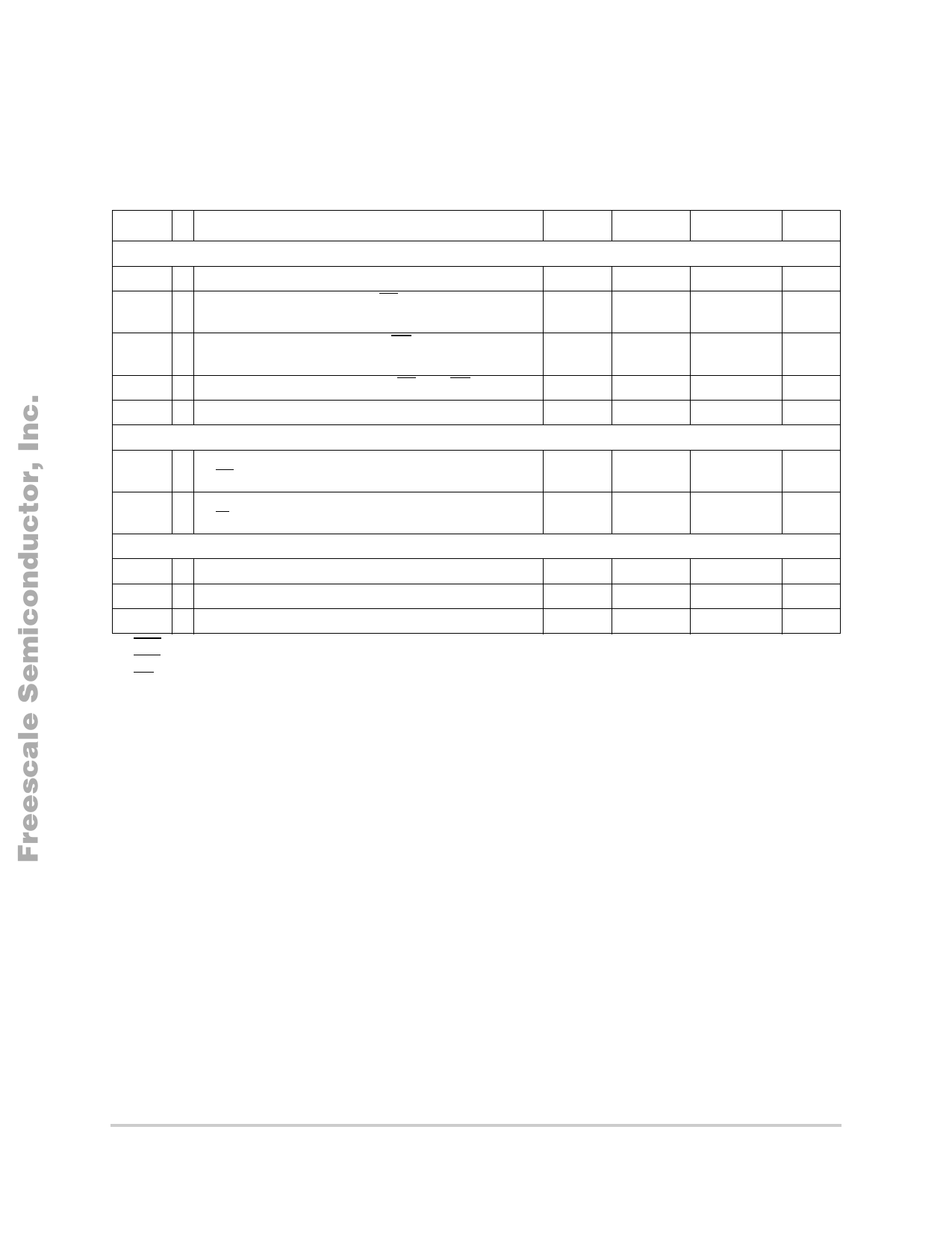
Table 23 lists processor bus output timings. Read/write bus timings listed in Table 23 are shown in Figure 7
and Figure 8.
Table 23. External Bus Output Timing Specifications
Num
L6a
L6b
C
Rating
Control Outputs
CLKOUT high to chip selects valid 1
CLKOUT high to byte select (BS[1:0]) valid 2
Symbol
tCHCV
tCHBV
Min
Max
Unit
—
0.5tCYC + 10 ns
—
0.5tCYC + 10 ns
L6c
CLKOUT high to output select (OE) valid 3
tCHOV
—
0.5tCYC + 10 ns
L7a
CLKOUT high to control output (BS[1:0], OE) invalid
tCHCOI 0.5tCYC + 2
—
ns
L7b
CLKOUT high to chip selects invalid
tCHCI 0.5tCYC + 2
—
ns
Address and Attribute Outputs
L8
CLKOUT high to address (ADDR[21:0]) and control
tCHAV
—
(R/W) valid
10
ns
L9
CLKOUT high to address (ADDR[21:0]) and control
tCHAI
2
(R/W) invalid
—
ns
Data Outputs
L10
CLKOUT high to data output (DATA[15:0]) valid
tCHDOV
—
L11
CLKOUT high to data output (DATA[15:0]) invalid
tCHDOI
2
L12
CLKOUT high to data output (DATA[15:0]) high impedance tCHDOZ
—
1 CSn transitions after the falling edge of CLKOUT.
2 BSn transitions after the falling edge of CLKOUT.
3 OE transitions after the falling edge of CLKOUT.
13
ns
—
ns
9
ns
20
MAC7100 Microcontroller Family Hardware Specifications
MOTOROLA
PRELIMINARY—SUBJECT TO CHANGE WITHOUT NOTICE
For More Information On This Product,
Go to: www.freescale.com
Share Link: 