AGB3301 데이터 시트보기 (PDF) - ANADIGICS
부품명
상세내역
제조사
AGB3301 Datasheet PDF : 16 Pages
| |||
AGB3301
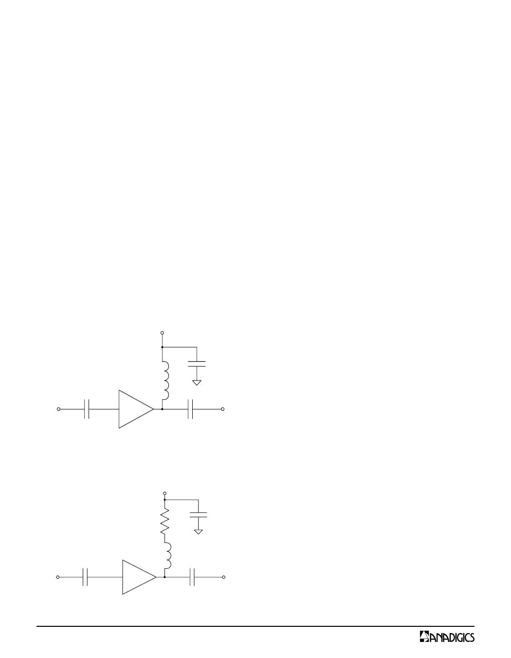
Bias Circuit
A schematic of the basic, unmatched bias circuit for the
AGB Series Gain Blocks is shown in Figure 33. The
RF input and output terminations are 50Ω. Inductor
L1 provides DC power from Vsupply and serves as an
RF choke to maintain desired AC performance. The
input capacitor C1 and output capacitor C2 are RF
blocks that isolate DC current from adjacent circuits.
Capacitor C3 is used as an RF bypass that minimizes
noise from the supply.
In some applications, a feedback resistor R1 may be
added in series with L1, as shown in Figure 34, for
improved stability or to serve as a voltage drop for
operation from higher supply voltages.
Matching for RF Performance
The AGB3301 Gain Block amplifier can be used in
many fixed wireless frequency bands, such as the
824-894 MHz U.S. cellular bands, the 1850-1990 MHz
PCS band, the 880-960 MHz GSM band, the 2400-
2500 MHz ISM band, and the 2500-2686 MHz MMDS
band. Reactive matching circuits may be designed for
VSUPPLY
both the input and output, in order to optimize the RF
performance for a particular application. For example,
gain, linearity (OIP3) and return loss may be improved
over a particular frequency band of interest.
Recommended matching circuits for various
applications, as well as wideband S-parameters to use
in the simulation of custom designs, are included in this
data sheet. For a particular application not addressed
in the data sheet, please consult with an ANADIGICS
Sales Reperesentative or Application Engineer.
Evaluation Boards
A versatile evaluation board that enables users
to measure actual device performance has been
developed for the AGB Series Gain Blocks. The
generic layout allows the user to implement a wide
variety of matching circuits, in order to assess
performance for a particular application.
The evaluation board is 1.0” square, and is fabricated
on 0.031” thick FR-4 material. Figures 35 and 36 show
the via hole locations and the layout pattern on both
sides of the evaluation board. The vias have a 0.010”
diameter and are plated through.
C3
L1
To request an evaluation board, please contact an
ANADIGICS Sales Reperesentative or Application
Engineer.
C1
C2
RF
Gain
RF
ESD Sensitivity
Input
Block
VDD
Output Electrostatic discharges can cause permanent damage
to this device. Electrostatic discharges accumulate
Figure 33: Unmatched Bias Circuit
on test equipment and the human body, and can
discharge without detection. Although the AGB3301
has some internal ESD protection, proper precautions
and handling are strongly recommended. Refer to the
VSUPPLY
ANADIGICS application note on ESD precautions.
C1
RF
Input
C3
R1
L1
Gain
Block
C2
VDD
RF
Output
S-Parameter Data
Table 11 depicts the raw Magnitude and Angle data
for an unmatched AGB3301 over the 50 to 3000 MHz
frequency range of operation. Data is shown in 100
MHz steps, with a characteristic impedance of 50
Ohms, Vdd = +9 V, and at Ta = +25 oC.
Figure 34: Bias Circuit with Optional
Feedback/Voltage Drop Resistor
12
Data Sheet - Rev 2.2
03/2012
Share Link: 