AS3930 데이터 시트보기 (PDF) - austriamicrosystems AG
부품명
상세내역
제조사
AS3930 Datasheet PDF : 32 Pages
| |||
AS3930
Datasheet - Detailed Description
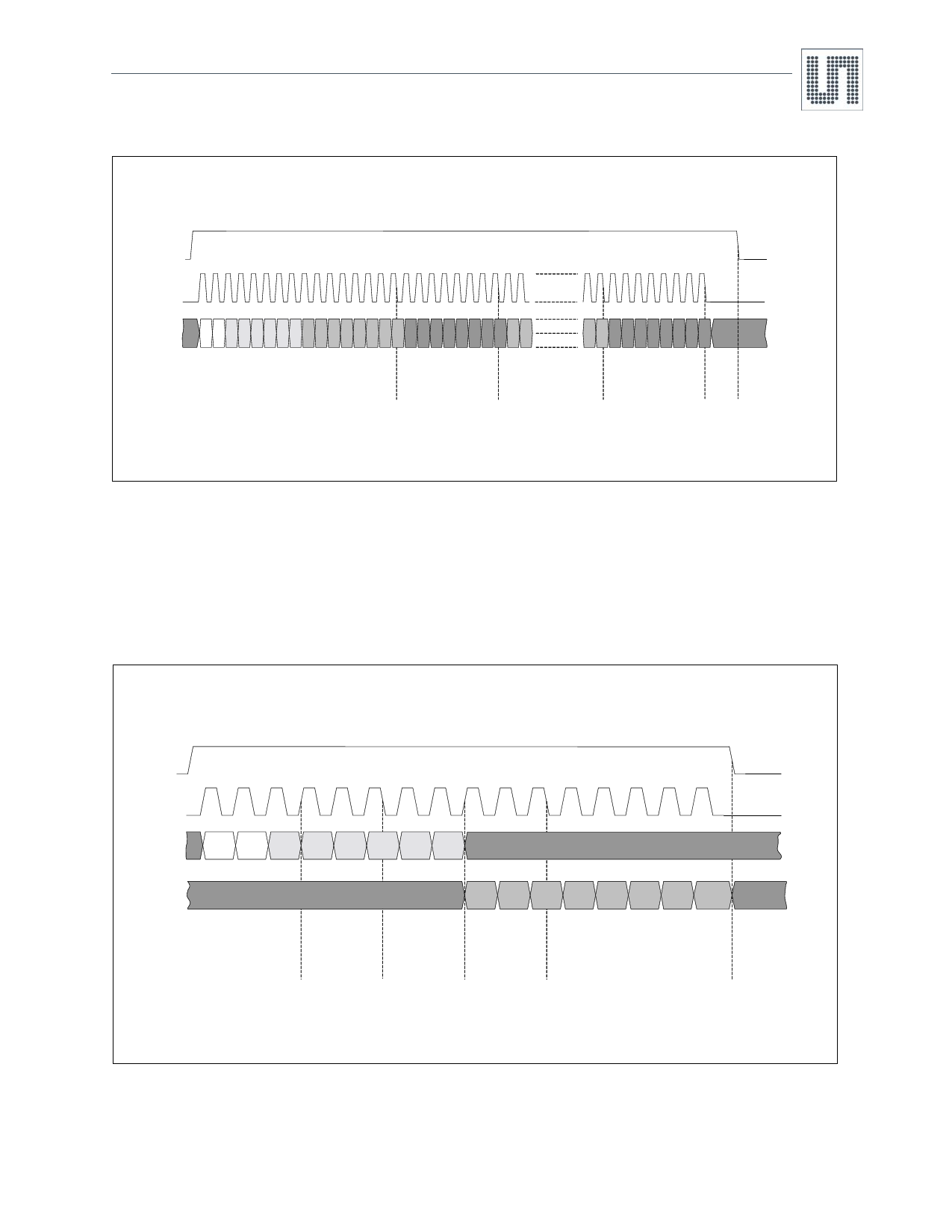
Figure 13. Writing of Register Data with Auto-incrementing Address
CS
SCLK
SDI
X
0
0
A
5
A
4
A
3
A
2
A
1
A
0
D
7
D
6
D
5
D
4
D
3
D
2
D
1
D
0
D
7
D
6
D
5
D
4
D
3
D
2
D
1
D
0
D
7
D
6
DDDDDDDDDD
1076543210
Two leading
Zeros indicate
WRITE Mode
Data is moved
to Address
<A5-A0 >
Data is moved
to Address
<A5-A0 > + 1
Data is moved
to Address
<A5-A0 > + (n-1)
Data is moved
to Address
<A5-A0 > + n
X
CS falling
edge signals
end of
WRITE Mode
Reading of Data from Addressable Registers (READ Mode). Once the address has been sent through SDI, the data can be fed
through the SDO pin out to the microcontroller.
A CS LOW toggling high-low-high has to be performed after finishing the read mode session, in order to indicate the end of the READ command
and prepare the Interface to the next command control Byte.
To transfer bytes from consecutive addresses, SDI master has to keep the CS signal high and the SCLK clock has to be active as long as data
need to be read.
Figure 14. Reading of a Single Register Byte
CS
SCLK
SDI
X 0 1 A5 A4 A3 A2 A1 A0
X
SDO
X
D7 D6 D5 D4 D3 D2 D1 D0
X
01 pattern
indicates
READ Mode
SCLK rising
edge Data is
transfered from
µC
SCLK
falling edge
Data is
sampled
SCLK rising
edge Data is
moved from
Address
<A5-A0>
SCLK falling
edge Data is
transfered to
µC
CS falling
edge signals
end of READ
Mode
www.ams.com/LF-Receiver/AS3930
Revision 1.5
16 - 32
Share Link: 