AT25FS040 데이터 시트보기 (PDF) - Atmel Corporation
부품명
상세내역
제조사
AT25FS040 Datasheet PDF : 25 Pages
| |||
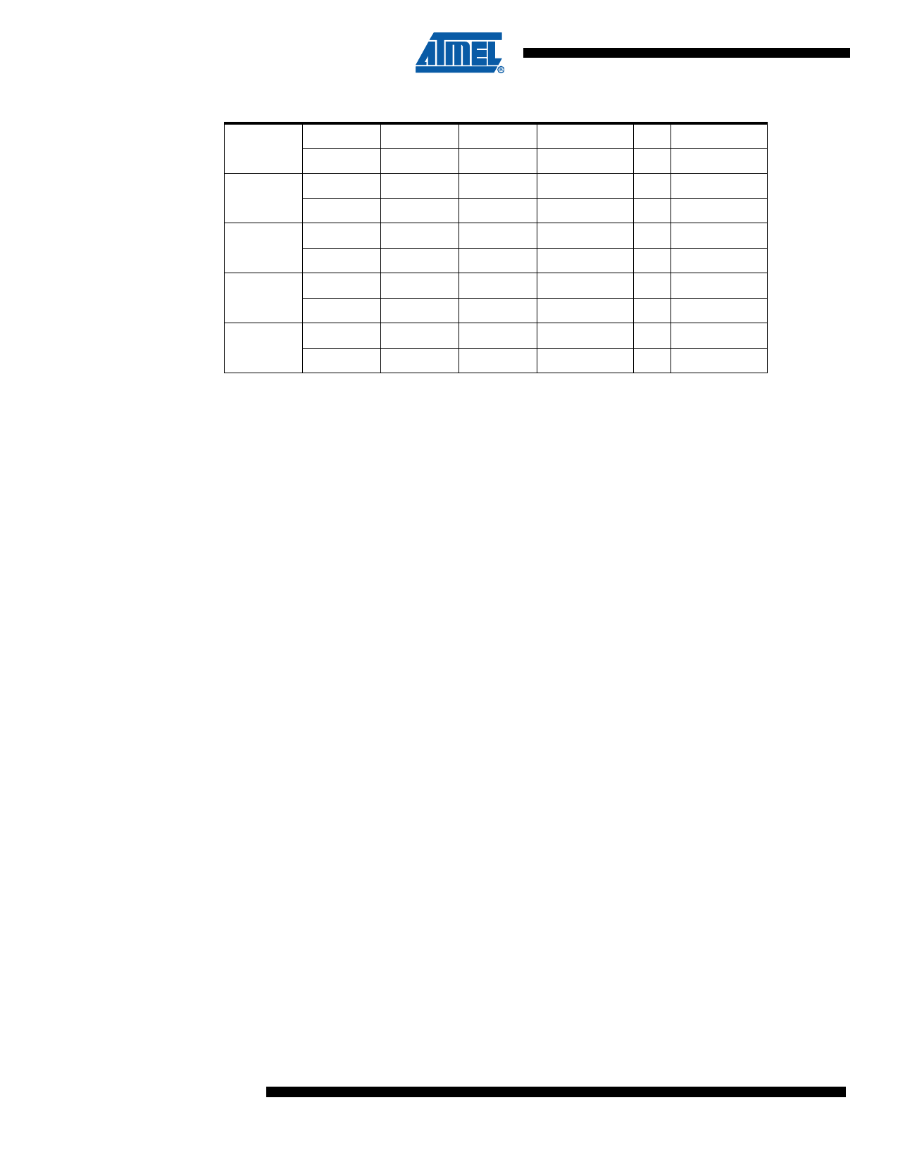
Table 4-8. Sector and Block Address (Continued)
Block 5
Block 4
Block 3
Block 2
Block 1
04FFFFH
040000H
03FFFFH
030000H
02FFFFH
020000H
01FFFFH
010000H
00FFFFH
000000H
BLOCK ERASE (BLOCK ERASE): The BLOCK ERASE instruction sets all 64K bytes in the
selected block to logic 1 or erased state. In order to block erase the AT25FS040, two sep-
arate instructions must be executed. First, the device must be write enabled via the
WREN instruction. Then the BLOCK ERASE instruction can be executed and will erase
every byte in the selected block if the block is not locked out. The block address is auto-
matically determined if any address within the block is selected (see Figure 5-11). The
BLOCK ERASE instruction is internally controlled and self timed to completion. During
this time, all commands will be ignored except RDSR instruction. The progress or com-
pletion of the erase operation can be determined by reading ready/busy bit (bit 0) through
RDSR instruction. If Bit 0=1, block erase cycle is in progress. If Bit0=0, the erase opera-
tion has been completed. The AT25FS040 will automatically return to the write disable
state at the completion of the BLOCK ERASE cycle.
CHIP ERASE (CHIP ERASE): As an alternative to the SECTOR ERASE/BLOCK ERASE, the
CHIP ERASE instruction will erase every byte in all sectors that are not locked out. First, the
device must be write enabled via the WREN instruction. Then the CHIP ERASE instruction can
be executed. The CHIP ERASE instruction is internally controlled; it will automatically be timed
to completion. The CHIP ERASE cycle time typically is 4 seconds. During the internal erase
cycle, all instructions will be ignored except RDSR. The AT25FS040 will automatically return to
the write disable state at the completion of the CHIP ERASE cycle.
14 AT25FS040
5107E–SFLSH–8/07
Share Link: 