ATA6626C(2014) 데이터 시트보기 (PDF) - Atmel Corporation
부품명
상세내역
제조사
ATA6626C Datasheet PDF : 29 Pages
| |||
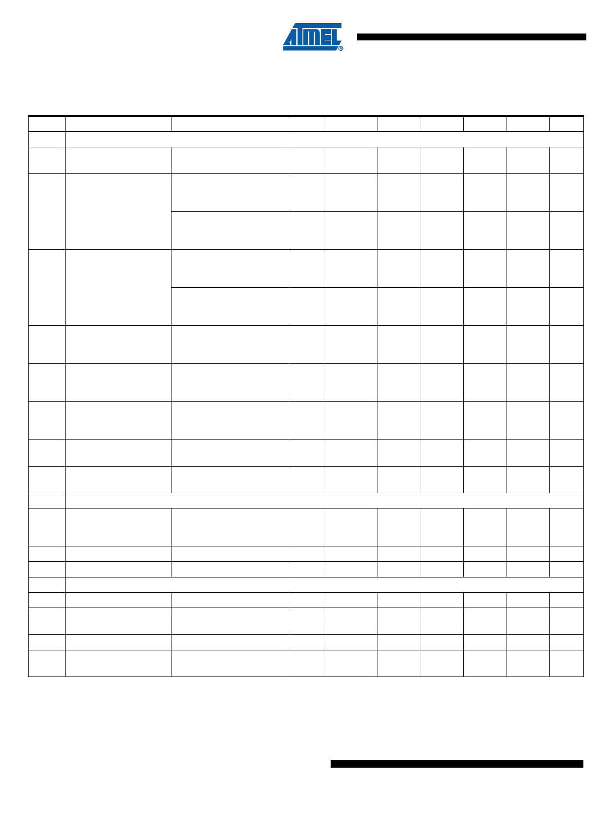
9. Electrical Characteristics (Continued)
5V < VS < 27V, -40°C < Tj < 150°C, unless otherwise specified. All values refer to GND pins
No. Parameters
Test Conditions
Pin Symbol Min.
Typ.
Max.
Unit
4 EN Input Pin
4.1 Low-level voltage input
4.2 High-level voltage input
EN
VENL
–0.3
EN
VENH
2
+0.8
V
VCC +
0.3V
V
4.3 Pull-down resistor
VEN = VCC
4.4 Low-level input current VEN = 0V
5 NTRIG Watchdog Input Pin
EN
REN
EN
IEN
50
125
200
kΩ
–3
+3
µA
5.1 Low-level voltage input
5.2 High-level voltage input
NTRIG
NTRIG
VNTRIGL
VNTRIGH
–0.3
2
+0.8
V
VCC +
0.3V
V
5.3 Pull-up resistor
5.4
High-level leakage
current
VNTRIG = 0V
VNTRIG = VCC
NTRIG RNTRIG
125
250
400
kΩ
NTRIG
INTRIG
–3
+3
µA
6 Mode Input Pin
6.1 Low-level voltage input
6.2 High-level voltage input
MODE
MODE
VMODEL
VMODEH
–0.3
2
+0.8
V
VCC +
0.3V
V
6.3 Leakage current
7 INH Output Pin
VMODE = VCC or
VMODE = 0V
MODE
IMODE
–3
+3
µA
7.1 High-level voltage
IINH = –15mA
INH
VINHH
VS –
0.75
VS
V
7.2
Switch-on resistance
between VS and INH
INH
RINH
30
50
Ω
7.3 Leakage current
Sleep Mode
VINH = 0V/27V, VS = 27V
INH
IINHL
–3
+3
µA
LIN Bus Driver: Bus Load Conditions:
8
Load 1 (Small): 1nF, 1kΩ; Load 2 (Large): 10nF, 500Ω; Internal Pull-up RRXD = 5kΩ; CRXD = 20pF
Load 3 (Medium): 6.8nF, 660Ω, Characterized on Samples
10.6 and 10.7 Specifies the Timing Parameters for Proper Operation at 20kBit/s and 10.8 and 10.9 at 10.4kBit/s
8.1
Driver recessive output
voltage
Load1/Load2
LIN
VBUSrec 0.9 × VS
VS
V
8.2
Driver dominant voltage
VVS = 7V
Rload = 500Ω
8.3
Driver dominant voltage
VVS = 18V
Rload = 500Ω
8.4
Driver dominant voltage
VVS = 7.0V
Rload = 1000Ω
8.5
Driver dominant voltage
VVS = 18V
Rload = 1000Ω
8.6 Pull-up resistor to VS
The serial diode is
mandatory
LIN
V_LoSUP
1.2
V
LIN
V_HiSUP
2
V
LIN
V_LoSUP_1k
0.6
V
LIN
V_HiSUP_1k
0.8
V
LIN
RLIN
20
30
60
kΩ
8.7
Voltage drop at the
serial diodes
In pull-up path with Rslave
ISerDiode = 10mA
LIN
VSerDiode
0.4
1.0
V
*) Type means: A = 100% tested, B = 100% correlation tested, C = Characterized on samples, D = Design parameter
Type*
A
A
A
A
A
A
A
A
A
A
A
A
A
A
A
A
A
A
A
A
D
18 ATA6622C/ATA6624C/ATA6626C [DATASHEET]
4986O–AUTO–10/14
Share Link: 