ATA6626 데이터 시트보기 (PDF) - Atmel Corporation
부품명
상세내역
제조사
ATA6626 Datasheet PDF : 31 Pages
| |||
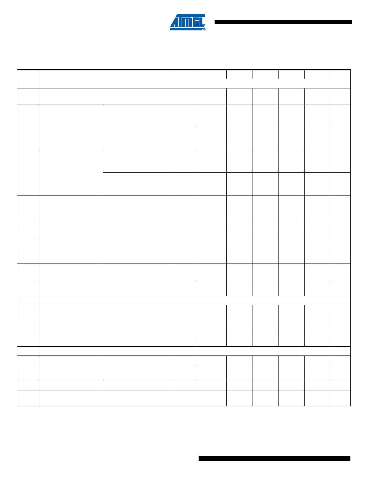
9. Electrical Characteristics
5V < VS < 27V, -40°C < Tj < 150°C, unless otherwise specified. All values refer to GND pins
No. Parameters
Test Conditions
Pin Symbol Min.
Typ.
Max.
Unit
1 VS Pin
1.1
Nominal DC voltage
range
VS
VS
5
27
V
Sleep Mode
VLIN > VS – 0.5V
1.2
Supply current in Sleep VS < 14V (Tj = 25°C)
Mode
Sleep Mode
VLIN > VS – 0.5V
VS < 14V (Tj = 125°C)
Bus recessive
VS < 14V (Tj = 25°C)
1.3
Supply current in Silent Without load at VCC
Mode
Bus recessive
VS < 14V (Tj = 125°C)
Without load at VCC
VS
IVSsleep
3
10
14
µA
VS
IVSsleep
5
11
16
µA
VS
IVSsi
47
57
67
µA
VS
IVSsi
56
66
76
µA
1.4
Supply current in Normal
Mode
Bus recessive
VS < 14V
Without load at VCC
VS
IVSrec
0.3
0.8
mA
1.5
Supply current in Normal
Mode
Bus dominant
VS < 14V
VCC load current 50 mA
1.6
Supply current in
Fail-safe Mode
Bus recessive
VS < 14V
Without load at VCC
VS
IVSdom
50
VS
IVSfail
250
53
mA
550
µA
1.7
VS undervoltage
threshold
VS
VSth
4.0
4.5
5
V
1.8
VS undervoltage
threshold hysteresis
VS
VSth_hys
0.2
V
2 RXD Output Pin
2.1
Low-level output sink
current
Normal Mode
VLIN = 0V
VRXD = 0.4V
2.2 Low-level output voltage IRXD = 1 mA
2.3 Internal resistor to VCC
3 TXD Input/Output Pin
RXD
IRXD
1.3
2.5
8
mA
RXD
VRXDL
RXD
RRXD
3
0.4
V
5
7
kΩ
3.1 Low-level voltage input
3.2 High-level voltage input
TXD
TXD
VTXDL
VTXDH
–0.3
2
+0.8
V
VCC +
0.3V
V
3.3 Pull-up resistor
3.4
High-level leakage
current
VTXD = 0V
VTXD = VCC
TXD
RTXD
125
250
400
kΩ
TXD
ITXD
–3
+3
µA
*) Type means: A = 100% tested, B = 100% correlation tested, C = Characterized on samples, D = Design parameter
Type*
A
A
A
A
A
A
A
A
A
A
A
A
A
A
A
A
A
18 ATA6622/ATA6624/ATA6626
4986I–AUTO–07/10
Share Link: 