BD5446EFV(2010) 데이터 시트보기 (PDF) - ROHM Semiconductor
부품명
상세내역
제조사
BD5446EFV Datasheet PDF : 31 Pages
| |||
BD5446EFV
Technical Note
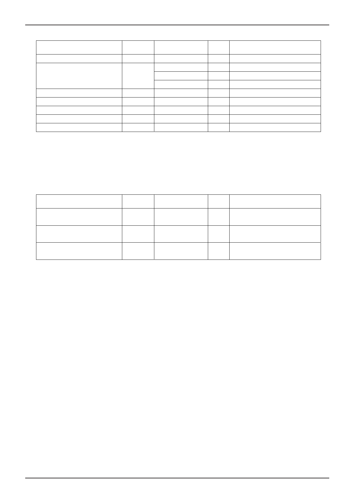
●Absolute maximum ratings (Ta=25℃)
Parameter
Symbol
Ratings
Unit
Supply voltage
VCC
30
V
2.0
W
Power dissipation
Pd
4.5
W
6.2
W
Input voltage
VIN
-0.3 ~ 4.5
V
Open-drain terminal voltage
VERR
-0.3 ~ 30
V
Operating temperature range
Topr
-25 ~ +85
℃
Storage temperature range
Tstg
-55 ~ +150
℃
Maximum junction temperature
Tjmax
+150
℃
*1 The voltage that can be applied reference to GND (Pin 6, 36, 37, 45, 46).
*2 Do not, however exceed Pd and Tjmax=150℃.
*3 70mm×70mm×1.6mm, FR4, 1-layer glass epoxy board (Copper on bottom layer 0%)
Derating in done at 16mW/℃ for operating above Ta=25℃.
*4 70mm×70mm×1.6mm, FR4, 2-layer glass epoxy board (Copper on bottom layer 100%)
Derating in done at 36mW/℃ for operating above Ta=25℃. There are thermal via on the board.
*5 70mm×70mm×1.6mm, FR4, 4-layer glass epoxy board (Copper on bottom layer 100%)
Derating in done at 49.6mW/℃ for operating above Ta=25℃. There are thermal via on the board.
Conditions
Pin 25, 28, 29, 53, 54
*3
*4
*5
Pin 7 ~ 18, 21
Pin24
*1 *2
*1
*1
●Operating conditions (Ta=25℃)
Parameter
Supply voltage
Minimum load impedance
(Speaker Output)
Minimum load impedance
(DAC Output)
*6 Do not, however exceed Pd.
* No radiation-proof design.
Symbol
VCC
RL_SP
RL_DA
Ratings
10 ~ 26
5.4
20
Unit
Conditions
V Pin 25, 28, 29, 53, 54
Ω *6
kΩ Pin 22, 23
*1 *2
www.rohm.com
© 2010 ROHM Co., Ltd. All rights reserved.
2/30
2010.05 - Rev.B
Share Link: 