LH168M 데이터 시트보기 (PDF) - Sharp Electronics
부품명
상세내역
제조사
LH168M Datasheet PDF : 17 Pages
| |||
LH168M
PRECAUTIONS
Precautions when connecting or disconnecting
the power supply
This IC has some power supply pins, so it may be
permanently damaged by a high current which may
flow if voltage is supplied to the LCD drive power
supply while the logic system power supply is
floating. Therefore, when connecting the power
supply, observe the following sequence.
VCC / logic input / VLS, VH0-VH64, VL0-VL64
When disconnecting the power supply, follow the
reverse sequence.
Reference voltage input
The relation of the reference voltage input is shown
here.
VLS > VH0 ≥ VH8 ≥ π ≥ VH56 ≥ VH64 ≥ 0.5VLS ≥
VL64 ≥ VL56 ≥ π ≥ VL8 ≥ VL0 > GND
Maximum ratings
When connecting or disconnecting the power
supply, this IC must be used within the range of the
absolute maximum ratings.
Target output load
This IC is designed for a 150 pF output load
capacity. When using this IC for other than 150 pF
panels, confirm the device is having no problem
before using it.
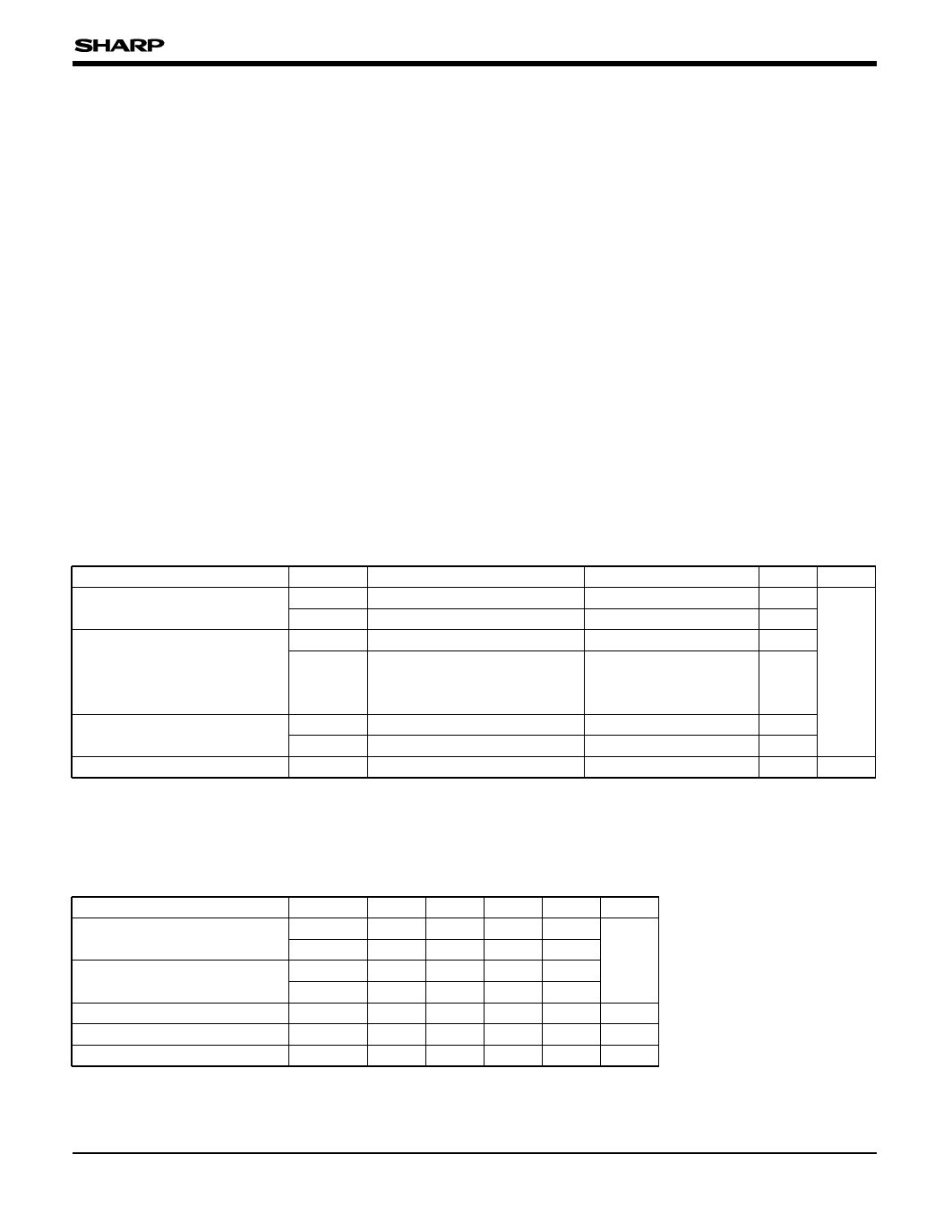
ABSOLUTE MAXIMUM RATINGS
PARAMETER
Supply voltage
Input voltage
Output voltage
Storage temperature
SYMBOL
APPLICABLE PINS
VCC
VCC
VLS
VLS
VI
VH0-VL0
SPIO, SPOI, CKP, CKN, LS,
VI REV, LBR, POL, X0P-X2N,
Y0P-Y2N, Z0P-Z2N
VO
SPIO, SPOI
VO
XO1-ZO128
TSTG
NOTES :
1. TA = +25 ˚C
2. The maximum applicable voltage on any pin with respect to GND (0 V).
RATING
–0.3 to +6.0
–0.3 to +13.0
–0.3 to VLS + 0.3
–0.3 to VCC + 0.3
–0.3 to VCC + 0.3
–0.3 to VLS + 0.3
–45 to +125
UNIT
V
V
V
NOTE
V
1, 2
V
V
˚C
RECOMMENDED OPERATING CONDITIONS
PARAMETER
Supply voltage
Reference voltage input
Clock frequency
SYMBOL MIN.
VCC
+3.0
VLS
+8.0
VH0-VH64 0.5VLS
VL0-VL64 +0.1
fCK
TYP.
MAX.
+3.6
+12.0
VLS – 0.1
0.5VLS
68
UNIT
V
V
V
V
MHz
LCD drive output load capacity CL
Operating temperature
TOPR
–20
150 pF
+75 ˚C
NOTE :
1. The applicable voltage on any pin with respect to GND (0 V).
NOTE
1
13
Share Link: 