EL2002 데이터 시트보기 (PDF) - Intersil
부품명
상세내역
제조사
EL2002 Datasheet PDF : 8 Pages
| |||
EL2002
Absolute Maximum Ratings (TA=25°C)
VS Supply Voltage (V+ - V-) . . . . . . . . . . . . . . . . . . . . ±18V or 36V
VIN Input Voltage . . . . . . . . . . . . . . . . . . . . . . . . . . . . .±15V or VS
If the input exceeds the ratings shown (or the supplies) or if the input to output
voltage exceeds ±7.5V then the input current must be limited to ±50mA. See
the applications section for more information.
IIN Input Current (See above note) . . . . . . . . . . . . . . . . . . . ±50mA
PD Power Dissipation . . . . . . . . . . . . . . . . . . . . . . . . . See Curves
The maximum power dissipation depends on package type, ambient
temperature and heat sinking. See the characteristic curves for more details.
Output Short Circuit Duration . . . . . . . . . . . . . . . . . . . . . Continuous
A heat sink is required to keep the junction temperature below the absolute
maximum when the output is short circuited.
TA Operating Temperature Range . . . . . . . . . . . . . 0°C to +75°C
TJ Operating Junction Temperature. . . . . . . . . . . . . . . . . . 150°C
TST Storage Temperature . . . . . . . . . . . . . . . . . .-65°C to +150°C
CAUTION: Stresses above those listed in “Absolute Maximum Ratings” may cause permanent damage to the device. This is a stress only rating and operation of the
device at these or any other conditions above those indicated in the operational sections of this specification is not implied.
IMPORTANT NOTE: All parameters having Min/Max specifications are guaranteed. Typical values are for information purposes only. Unless otherwise noted, all tests
are at the specified temperature and are pulsed tests, therefore: TJ = TC = TA
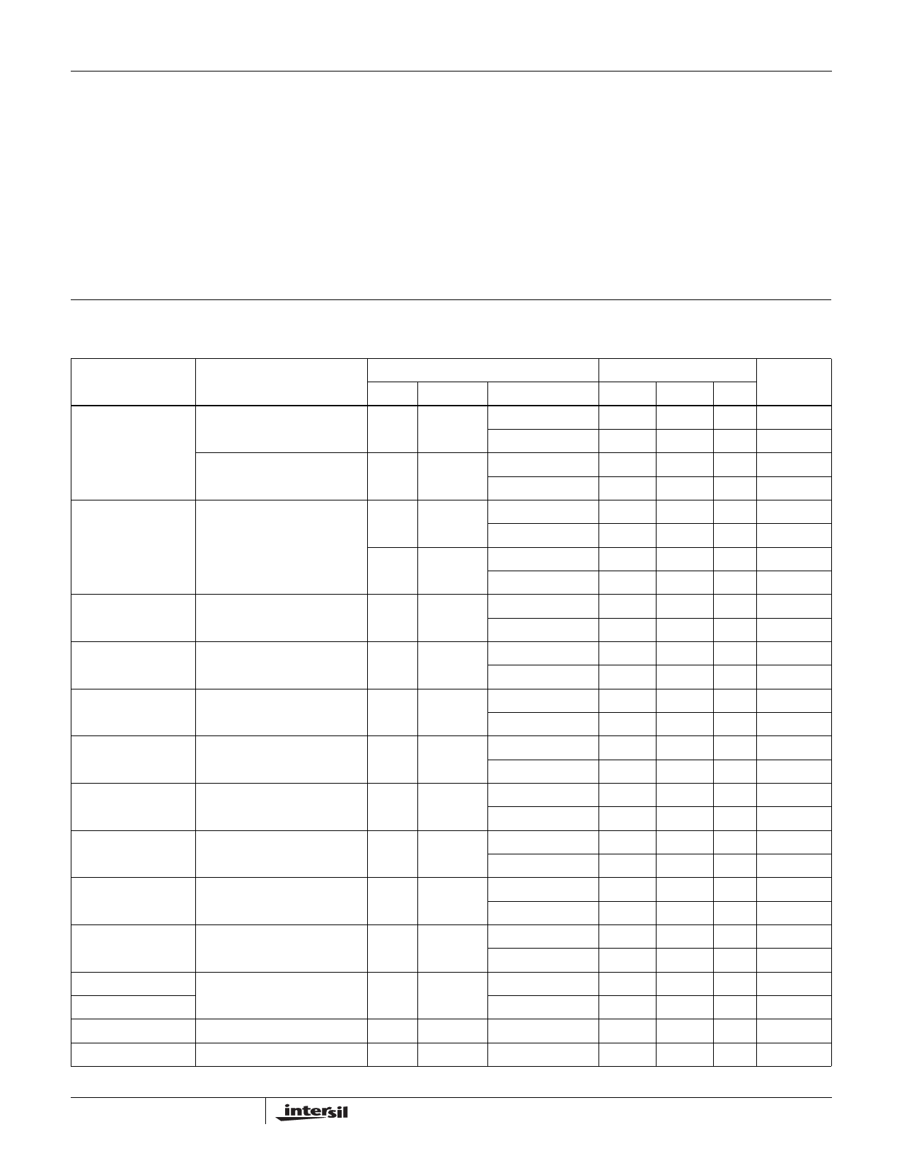
Electrical Specifications VS= ±15V, RS = 50Ω, unless otherwise specified.
PARAMETER
DESCRIPTION
TEST CONDITIONS
VIN
LOAD
TEMP
LIMITS
MIN
TYP
MAX
UNITS
VOS
Offset Voltage
0
∞
25°C
-15
5
+15
mV
TMIN, TMAX
-20
+20
mV
0
∞
25°C
-40
10
+40
mV
IIN
Input Current
0
∞
0
∞
TMIN, TMAX
-50
+50
mV
25°C
-10
3
+10
µA
TMIN, TMAX
-15
+15
µA
25°C
-15
5
+15
µA
RIN
AV1
AV2
AV3
VO
ROUT
IOUT
IS
PSRR
Input Resistance
Voltage Gain
Voltage Gain
Voltage Gain
with VS = ±5V
Output Voltage Swing
Output Resistance
Output Current
Supply Current
Supply Rejection (Note 2)
TMIN, TMAX
-20
+20
µA
+12V
100Ω
25°C
1
3
MΩ
TMIN, TMAX
0.1
MΩ
±12V
∞
25°C
0.990 0.998
V/V
TMIN, TMAX
0.985
V/V
±10V
100Ω
25°C
0.85
0.93
V/V
TMIN, TMAX
0.83
V/V
±3V
100Ω
25°C
0.83
0.91
V/V
TMIN, TMAX
0.80
V/V
±12V
100Ω
25°C
±10
±11
V
TMIN, TMAX
±9.5
V
±2V
100Ω
25°C
8
13
Ω
TMIN, TMAX
15
Ω
±12V (Note 1)
25°C
+100
+160
mA
0
∞
TMIN, TMAX
±95
mA
25°C
5
7.5
mA
0
∞
TMIN, TMAX
10
mA
25°C
60
75
dB
TMIN, TMAX
50
dB
tR
Rise Time
0.5V
100Ω
25°C
2.8
ns
tD
Propagation Delay
0.5V
100Ω
25°C
1.5
ns
2
Share Link: 