KM4110IT5TR3 데이터 시트보기 (PDF) - Fairchild Semiconductor
부품명
상세내역
제조사
KM4110IT5TR3 Datasheet PDF : 11 Pages
| |||
DATA SHEET
KM4110/KM4120
G=5
Output
Input
Refer to the evaluation board layouts shown in Figure 7
for more information.
Evaluation Board Information
The following evaluation boards are available to aid
in the testing and layout of this device:
Eval Board
KEB002
Description
Products
Single Channel,
KM4110IT5,
Dual Supply 5 & 6 lead SOT23 KM4120IT6
Time (200ns/div)
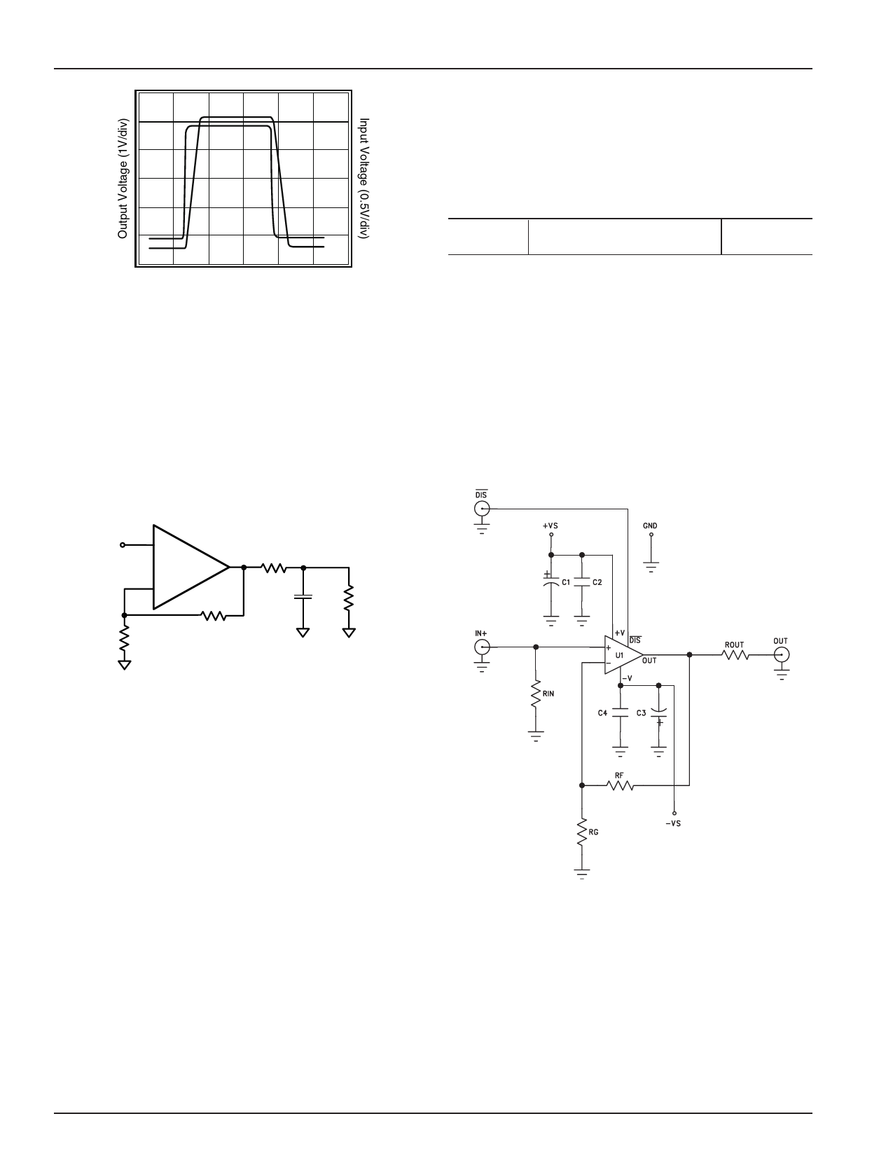
Figure 4: Overdrive Recovery
Driving Capacitive Loads
The Frequency Response vs. CL plot on page 4,
illustrates the response of the KM4110 and KM4120. A
small series resistance (Rs) at the output of the amplifier,
illustrated in Figure 5, will improve stability and
settling performance. Rs values in the Frequency
Response vs. CL plot were chosen to achieve maximum
bandwidth with less than 1dB of peaking. For maximum
flatness, use a larger Rs.
Evaluation board schematics and layouts are shown in
Figure 6 and Figure 7.
The KEB002 evaluation board is built for dual supply
operation. Follow these steps to use the board in a
single supply application:
1. Short -Vs to ground
2. Use C3 and C4, if the -Vs pin of the KM4110 or
KM4120 is not directly connected to the
ground plane.
+
-
Rf
Rg
Rs
CL RL
Figure 5: Typical Topology for driving
a capacitive load
Layout Considerations
General layout and supply bypassing play major roles
in high frequency performance. Fairchild has evaluation
boards to use as a guide for high frequency layout
and to aid in device testing and characterization.
Follow the steps below as a basis for high frequency
layout:
s Include 6.8µF and 0.01µF ceramic capacitors
s Place the 6.8µF capacitor within 0.75 inches
of the power pin
s Place the 0.01µF capacitor within 0.1 inches
of the power pin
s Remove the ground plane under and around the
part, especially near the input and output pins to
reduce parasitic capacitance
s Minimize all trace lengths to reduce
series inductances
Figure 6: Evaluation Board Schematic
8
REV. 1A February 2001
Share Link: 