EL4101C 데이터 시트보기 (PDF) - Elantec -> Intersil
부품명
상세내역
제조사
EL4101C Datasheet PDF : 6 Pages
| |||
EL4101C - Preliminary
500MHz Video Front End - 4:1MUX + DC-Restore
Absolute Maximum Ratings (TA = 25°C)
Values beyond absolute maximum ratings can cause the device to be pre-
maturely damaged. Absolute maximum ratings are stress ratings only
and functional device operation is not implied.
Supply Voltage (VS+ to VS-)
11V
Input Voltage
VS- - 0.3V, VS+ +0.3V
Storage Temperature Range
Ambient operating Temperature
Operating Junction Temperature
Power Dissipation
-65°C to +150°C
-40°C to +85°C
125°C
See Curves
Important Note:
All parameters having Min/Max specifications are guaranteed. Typ values are for information purposes only. Unless otherwise noted, all tests are at the
specified temperature and are pulsed tests, therefore: TJ = TC = TA.
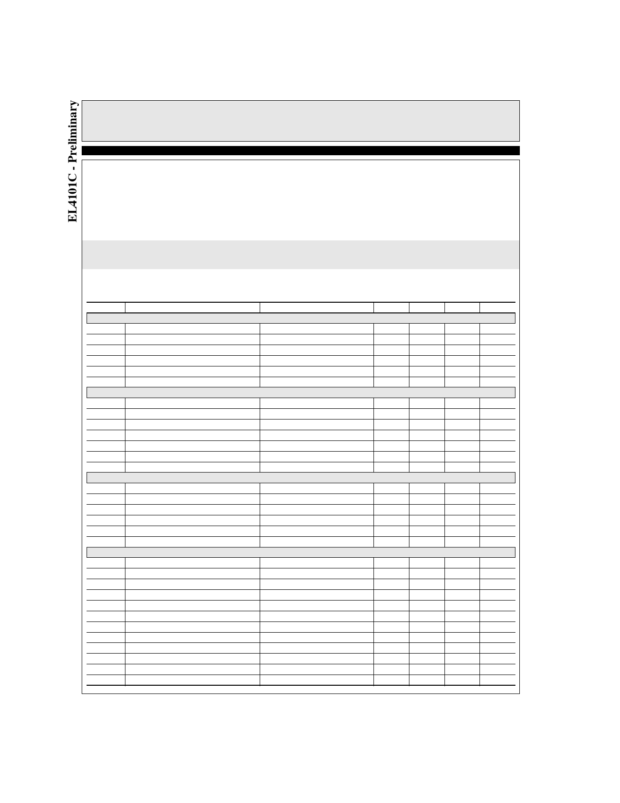
Electrical Characteristics
VS1+ = VS2+ = 5V, VS1- = VS2- = -5V, RFV = RGV = RFM = RGM =375, RLV = RLM = 150Ω, CLV = CLM = 3p, CH = 0.33n, GAIN = 2.
Parameter
Parameter Description
Conditions
Min
Typ
Max
Supply
IS1+
Positive Supply Current 1
IS-
Negative Supply Current
IS2+
Positive Supply Current 2
IS1S+
Positive Supply Current 1 in Standby
ISS-
Negative Supply Current in Standby
IS2S+
Input
Positive Supply Current 2 in Standby
IB
Input Bias Current
IBO
Input Bias Current Drift with Temp.
VIH
Input High Voltage
VIL
Input Low Voltage
IIL
Low Input Current for D0, D1, PDWN, HOLD
IIH
High Input Current for D0, D1, PDWN, HOLD
tSH
Sample and Hold Delay Time
Output
VOSM
VOS
δVOS
Output Offset Voltage - Monitor
DC-restore Offset Voltage
Output Offset Voltage Drift - Video
VOH
Output Voltage Swing, Pos.
VOL
Output Voltage Swing, Neg.
ISC
Output Short Circuit Current
AC Performance
SR
Slew Rate - Video Out (20%-80%)
SRM
Slew Rate - Monitor Out (20%-80%)
OS
Output Overshoot, Video
OSM
Output Overshoot, Monitor
tS
Settling Time to 1%, Video
tSM
Settling Time to 1%, Monitor
VREF
DC-restore -Reference Voltage Range
tSD
VOHS
DC-restore - Settling Time to 1%
DC-restore - Video Output Hold Step
VOSB
ICCL
DC-restore - Offset vs. Black Level
DC-restore - Charge Current Limit, ICAP
IDC
DC-restore - Droop Current, ICAP
VIN = 0, IL = 0
Standby
Standby
Standby
VIN = 0V
VIN = 0V
VIN = 0V
VIN =5V
VIN = 0V
Auto-zero on, DCREF = 0
Auto-zero on
AV = +1, monitor & video outputs
AV = +1, monitor & video outputs
RL = 10Ω, source or sink
VOUT = 4VP-P
VOUT = 4VP-P
VOUT = 1VP-P
VOUT = 1VP-P
Hold mode
VIN = -2V to +2V
Sample mode on
S - H transition
Sample mode on
Sample mode on
Hold mode on
-22.4
2
25
0
-400
-5
3.44
-3.43
65
1000
1250
-2
-1
210
-30
25
38
15
3.8
2
236
-2.2
TBD
48
-
12
18
-
TBD
3.5
-3.5
100
2100
2100
TBD
TBD
10
10
-
2.5
-0.5
-0.6
260
-
6.1
0.8
75
10
420
5
140
4500
3900
2
1
345
30
Unit
mA
mA
mA
mA
mA
µA
µA
nA/°C
V
V
µA
µA
ns
mV
mV
µV/°C
V
V
mA
V/µs
V/µs
%
%
ns
ns
V
µs
mV
mV/V
µA
nA
2
Share Link: 