LCX020 데이터 시트보기 (PDF) - Sony Semiconductor
부품명
상세내역
제조사
LCX020 Datasheet PDF : 24 Pages
| |||
LCX020BK
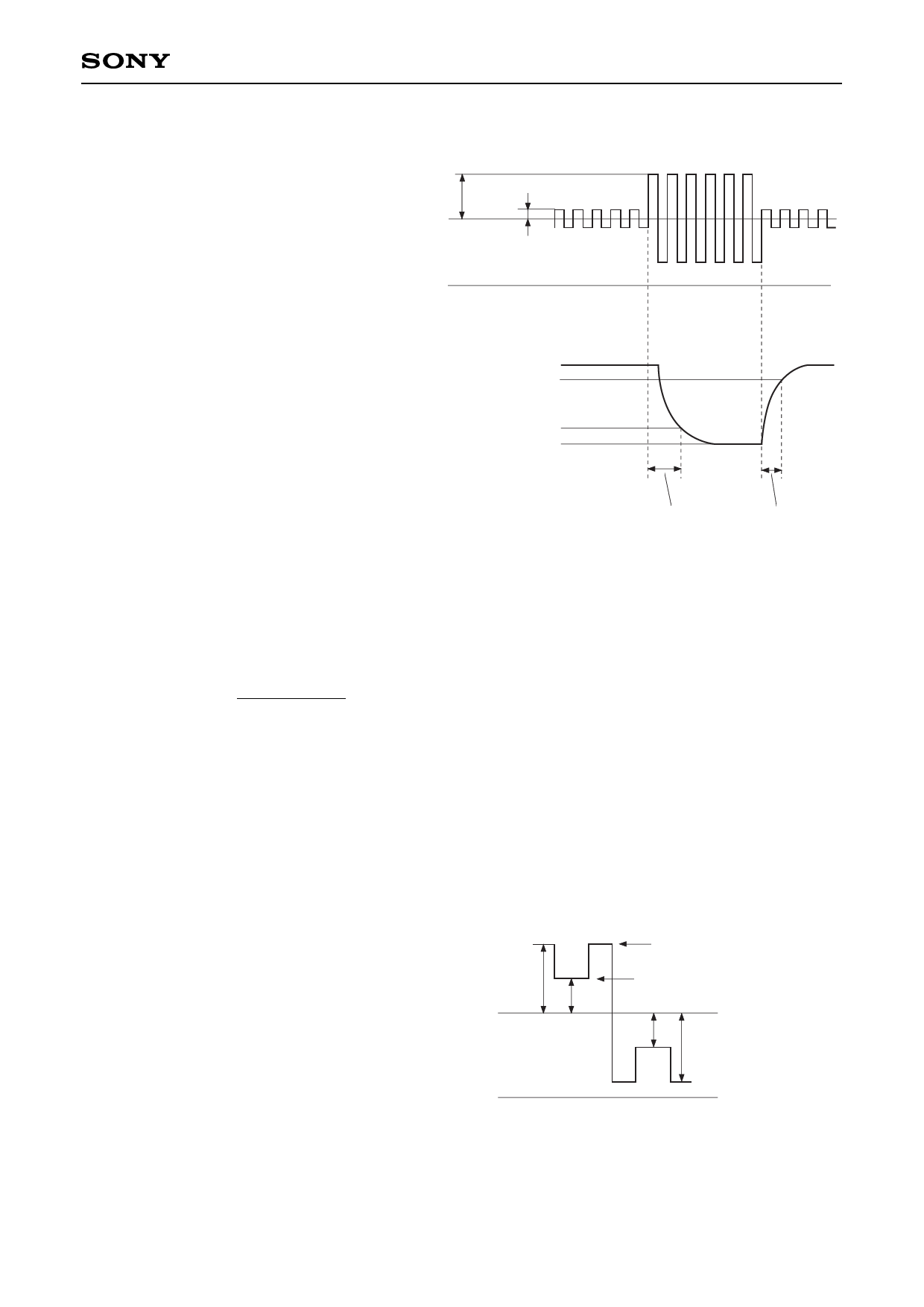
6. Response Time
Response time ton and toff are defined
by formulas (5) and (6) respectively.
ton = t1 – tON ... (5)
toff = t2 – tOFF ... (6)
t1: time which gives 10% transmittance
of the panel.
t2: time which gives 90% transmittance
of the panel.
The relationships between t1, t2, tON
and tOFF are shown in the right figure.
Input signal voltage (Waveform applied to the measured pixels)
4.5V
7.0V
0.5V
0V
Optical transmittance output waveform
100%
90%
10%
0%
tON t1
ton
tOFF t2
toff
7. Flicker
Flicker (F) is given by the formula (7). DC and AC (MAC16/SVGA/VGA/PC98/NTSC: 30Hz, rms, PAL:
25Hz, rms) components of the panel output signal for gray raster∗ mode are measured by a DC voltmeter
and a spectrum analyzer in System II.
F [dB] = 20log { AC component } ... (7)
DC component
∗ R, G, B input signal voltage for gray raster mode is given by
Vsig = 7.0 ± V50 [V]
where: V50 is the signal amplitude which gives 50% of
8. Image Retention Time
transmittance in V-T curve.
Image retention time is given by the following procedures.
Apply a monoscope signal to the LCD panel for 60 minutes and then change this signal to the gray scale of
Vsig = 7.0 ± VAC [V] (VAC: 3 to 4V) so as to give the maximum image retention. Hold input signal VAC. The
time for the residual image to disappear gives the image retention time.
∗ Monoscope signal conditions
Vsig = 7.0 ± 4.5 or 7.0 ± 2.0 [V]
(shown in the right figure)
Vcom = 6.6V
4.5V
7.0V
Black level
2.0V
White level
2.0V
4.5V
0V
Vsig waveform
– 14 –
Share Link: 