IS61VPD51236-200BI 데이터 시트보기 (PDF) - Integrated Silicon Solution
부품명
상세내역
제조사
IS61VPD51236-200BI
Integrated Silicon Solution

IS61VPD51236-200BI Datasheet PDF : 24 Pages
| |||
IS61VPD51232 IS61VPD51236 IS61VPD10018
CAPACITANCE(1,2)
Symbol
CIN
COUT
Parameter
Input Capacitance
Input/Output Capacitance
Conditions
VIN = 0V
VOUT = 0V
Max.
6
8
Notes:
1. Tested initially and after any design or process changes that may affect these parameters.
2. Test conditions: TA = 25°C, f = 1 MHz, Vcc = 3.3V.
Unit
pF
pF
ISSI ®
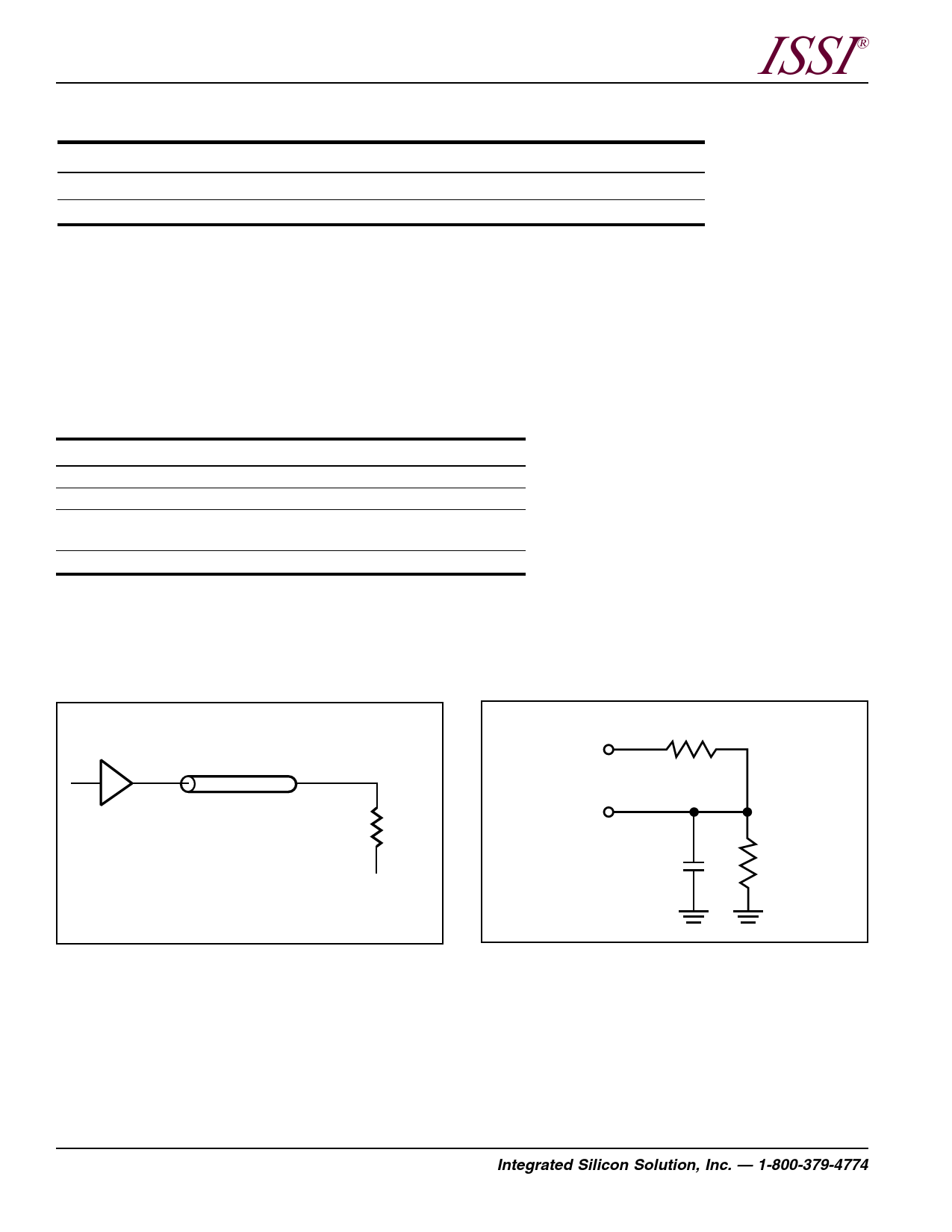
AC TEST CONDITIONS
Parameter
Input Pulse Level
Input Rise and Fall Times
Input and Output Timing
and Reference Level
Output Load
Unit
0V to 2.5V
1.5 ns
VCCQ/2V
See Figures 1 and 2
AC TEST LOADS
ZO = 50Ω
Output
Buffer
Figure 1
50Ω
VCCQ/2V
2.5V
1667 Ω
OUTPUT
5 pF
Including
jig and
scope
Figure 2
1538 Ω
10
Integrated Silicon Solution, Inc. — 1-800-379-4774
ADVANCE INFORMATION Rev. 00B
09/25/01
Share Link: