M58LW032A 데이터 시트보기 (PDF) - STMicroelectronics
부품명
상세내역
제조사
M58LW032A Datasheet PDF : 61 Pages
| |||
M58LW032A
Synchronous Bus Operations
For synchronous bus operations refer to Table 3
together with the text below.
Synchronous Burst Read. Synchronous Burst
Read operations are used to read from the memo-
ry at specific times synchronized to an external ref-
erence clock. The burst type, length and latency
can be configured. The different configurations for
Synchronous Burst Read operations are de-
scribed in the Burst Configuration Register sec-
tion.
A valid Synchronous Burst Read operation begins
when the address is set on the Address Inputs,
Write Enable is High, VIH, and Chip Enable and
Latch Enable are Low, VIL, during the active edge
of the Clock. The address is latched on the first ac-
tive clock edge when Latch Enable is low, or on
the rising edge of Latch Enable, whichever occurs
first. The data becomes available for output after
the X-latency specified in the Burst Control Regis-
ter has expired. The output buffers are activated
by setting Output Enable Low, VIL. See Figures 6
and 7 for examples of Synchronous Burst Read
operations.
In Continuous Burst mode one Burst Read opera-
tion can access the entire memory sequentially. If
the starting address is not associated with a page
(4 Word) boundary the Valid Data Ready, R, out-
put goes Low, VIL, to indicate that the data will not
be ready in time and additional wait-states are re-
quired. The Valid Data Ready output timing (bit
M8) can be changed in the Burst Configuration
Register.
The Synchronous Burst Read timing diagrams
and AC Characteristics are described in the AC
and DC Parameters section. See Figures 18, 19
and Table 20.
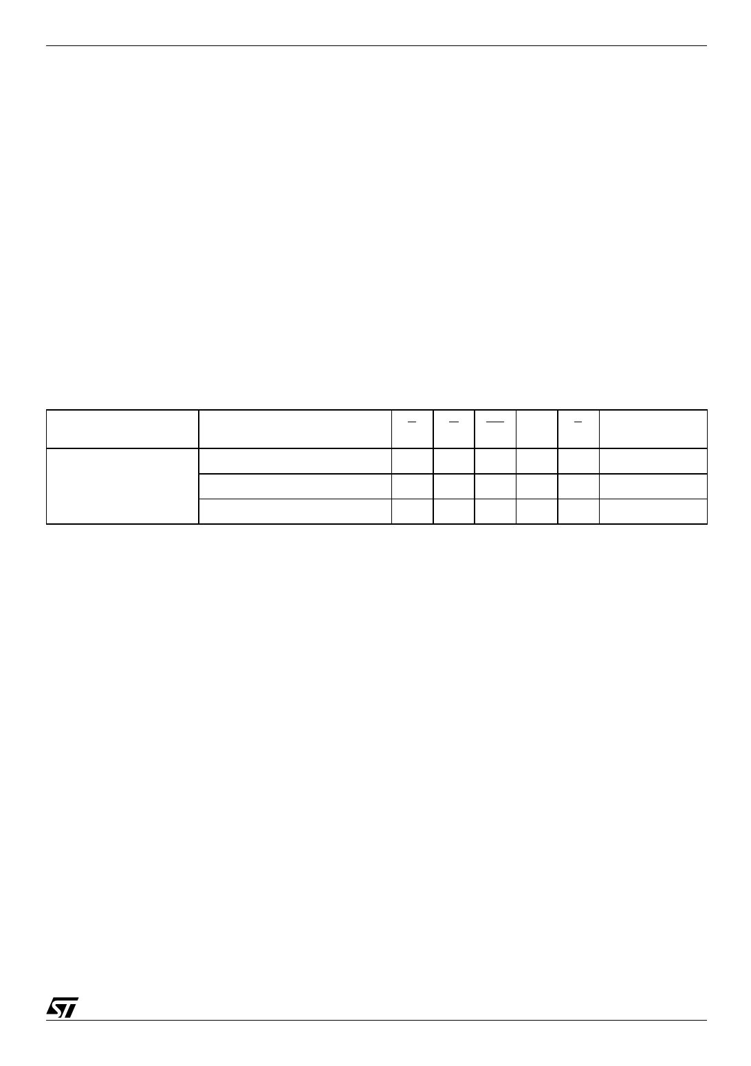
Table 3. Synchronous Burst Read Bus Operations
Bus Operation
Step
E
G
RP K(3)
L
Address Latch
VIL
X
VIH
T
VIL
Synchronous Burst Read Read
VIL VIL VIH
T
X
Read Abort
VIH
X
VIH
X
X
Note: 1. X = Don't Care, VIL or VIH.
2. M15 = 0, Bit M15 is in the Burst Configuration Register.
3. T = transition, see M6 in the Burst Configuration Register for details on the active edge of K.
A1-A21
DQ0-DQ15
Address Input
Data Output
High Z
15/61
Share Link: 