MAX98304EWL 데이터 시트보기 (PDF) - Maxim Integrated
부품명
상세내역
제조사
MAX98304EWL Datasheet PDF : 12 Pages
| |||
MAX98304
Mono 3.2W Class D Amplifier
ABSOLUTE MAXIMUM RATINGS
PVDD, IN+, IN-, SHDN, GAIN to PGND...................-0.3V to +6V
All Other Pins to PGND..........................-0.3V to (VPVDD + 0.3V)
Continuous Current Into/Out of PVDD, PGND, OUT_.... Q750mA
Continuous Input Current (all other pins)......................... Q20mA
Duration of Short Circuit Between
OUT_ and PVDD, PGND........................................Continuous
OUT+ and OUT-.....................................................Continuous
Continuous Power Dissipation (TA = +70NC) for Multilayer Board
9-Bump WLP (derate 10.6mW/NC)...............................848mW
Junction Temperature......................................................+150NC
Operating Temperature Range........................... -40NC to +85NC
Storage Temperature Range............................. -65NC to +150NC
Soldering Temperature (reflow).......................................+260NC
Stresses beyond those listed under “Absolute Maximum Ratings” may cause permanent damage to the device. These are stress ratings only, and functional
operation of the device at these or any other conditions beyond those indicated in the operational sections of the specifications is not implied. Exposure to absolute
maximum rating conditions for extended periods may affect device reliability.
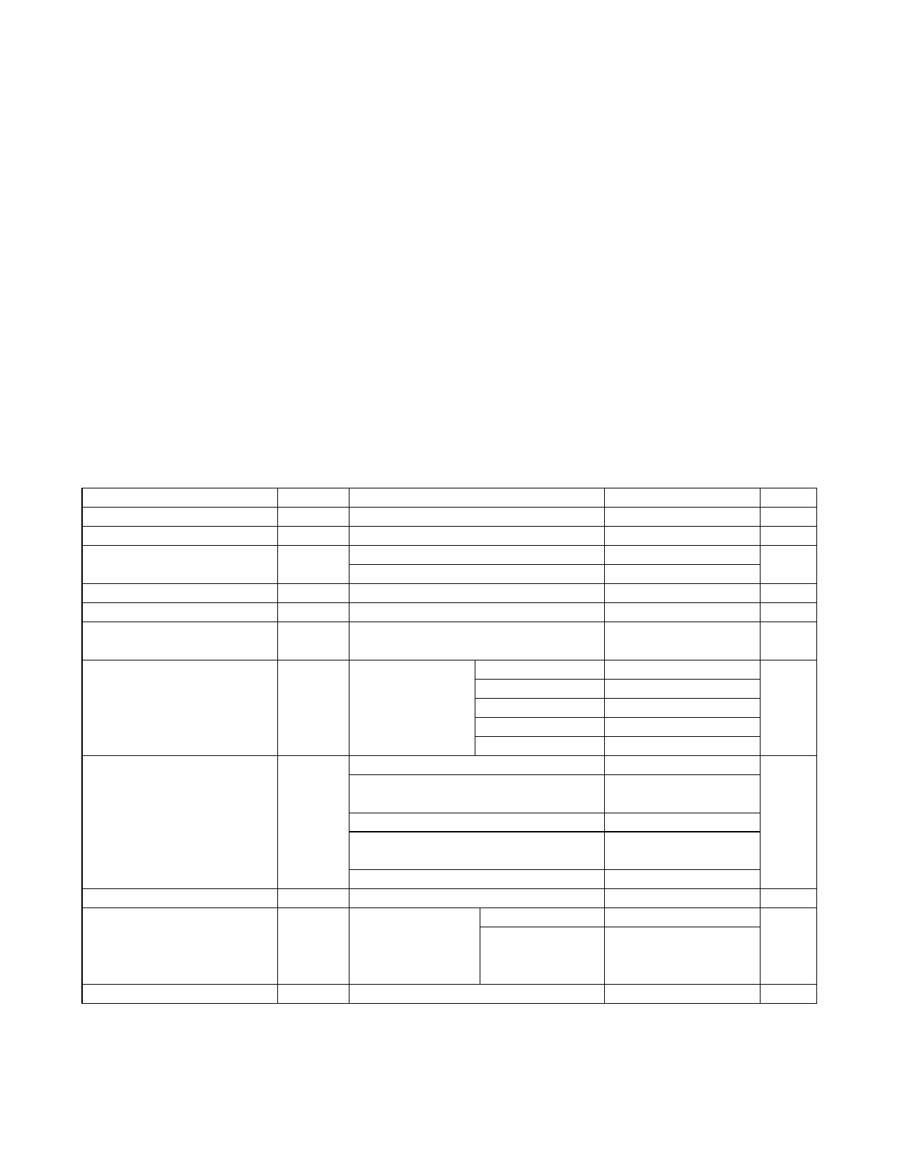
ELECTRICAL CHARACTERISTICS
(VPVDD = VSHDN = 5.0V, VPGND = 0V, AV = 12dB (GAIN = PGND), RL = J, RL connected between OUT+ to OUT-, AC measurement
bandwidth 20Hz to 22kHz, TA = TMIN to TMAX, unless otherwise noted. Typical values are at TA = +25NC.) (Notes 1, 2)
PARAMETER
Supply Voltage Range
Undervoltage Lockout
Quiescent Supply Current
Shutdown Supply Current
Turn-On Time
Bias Voltage
SYMBOL
CONDITIONS
PVDD Inferred from PSRR test
UVLO PVDD falling
IDD
TA = +25NC
VPVDD = 3.7V
ISHDN VSHDN = 0V, TA = +25NC
tON
VBIAS
MIN TYP MAX UNITS
2.5
5.5
V
1.5
1.8
2.2
V
1.2
1.8
mA
0.95
< 0.1 10
FA
3.4
10
ms
VPVDD
/2
V
Input Resistance
AV = 12dB
RIN
TA = +25°C,
single-ended
AV = 9dB
AV = 6dB
AV = 3dB
AV = 0dB
Connect GAIN to PGND
45
70
64
100
90
140
kI
128 200
180 280
11.5
12
12.5
Connect GAIN to PGND
through 100kI ±5%
8.5
9
9.5
Voltage Gain
AV Connect GAIN to PVDD
Connect GAIN to PVDD
through 100kI ±5%
5.5
6
6.5
dB
2.5
3
3.5
Output Offset Voltage
Click and Pop
GAIN unconnected
VOS TA = +25°C (Note 3)
Peak voltage,
Into shutdown
KCP
A-weighted, 32
samples per second, Out of shutdown
RL = 8I (Notes 3, 4)
-0.5
0
+0.5
Q1
Q4.5
mV
-74
dBV
-60
Common-Mode Rejection Ratio
CMRR fIN = 1kHz, input referred
80
dB
2
Maxim Integrated
Share Link: 