TDA8786G/C1 데이터 시트보기 (PDF) - Philips Electronics
부품명
상세내역
제조사
TDA8786G/C1 Datasheet PDF : 28 Pages
| |||
Philips Semiconductors
10-bit analog-to-digital interface for
CCD cameras
Product specification
TDA8786; TDA8786A
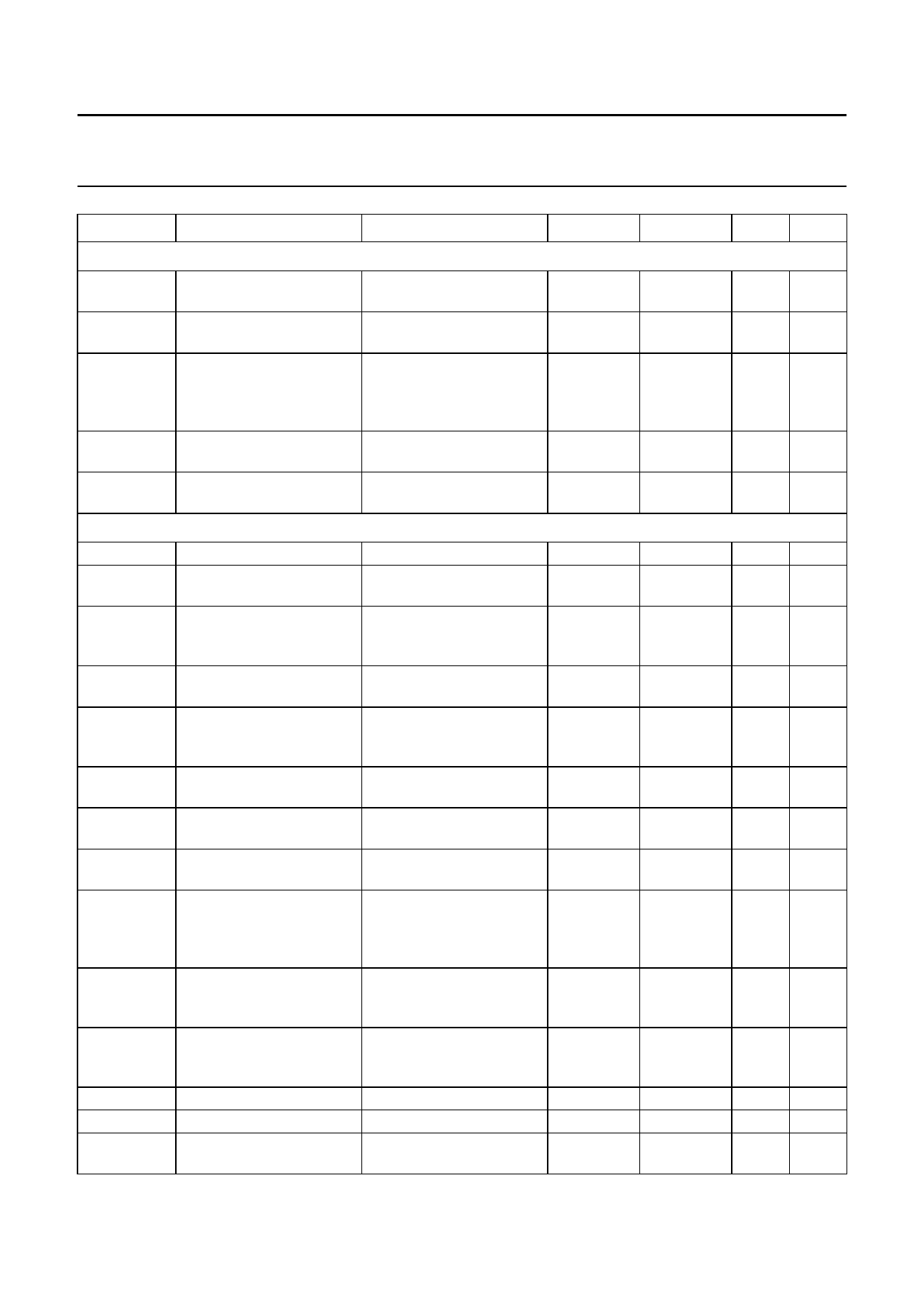
SYMBOL
PARAMETER
CONDITIONS
MIN.
Correlated Double Sampling; CDS
Vi(CDS)(p-p) CDS input amplitude
−
(peak-to-peak value)
ISTGE,IN1,IN2 input current pins 19, 46
−2
and 47
tCDS(min)
CDS control pulses
minimum active time
(HIGH for TDA8786,
LOW for TDA8786A)
fi(CDS1,2) = fCLK(pix)
12
Vi(CDS)(p-p) = 1200 mV
black-to-white transition in
one pixel (±1 LSB typ.)
thd1
hold time IN1 compared to see Fig.15
−
control pulse CDSP1
thd2
hold time of IN2 compared see Fig.15
−
to control pulse CDSP2
Amplifier outputs
GAMPOUT
output amplifier gain
−
ZAMPOUT
output amplifier
−
impedance
VAMPOUT(p-p) output amplifier dynamic
−
voltage level
(peak-to-peak value)
VAMPOUT(bl) output amplifier black
−
level voltage
VAGCOUT(p-p) AGC output amplifier
−
dynamic voltage level
(peak-to-peak value)
VAGCOUT
AGC output amplifier black
−
level voltage
ZAGCOUT
AGC output amplifier
at 10 kHz
−
output impedance
IAGCOUT
AGC output static drive static
−
current
VOPB(p-p)
optical black clamp and
−
blanking block output
dynamic voltage
(peak-to-peak value)
VOPB
optical black clamp and
−
blanking block output black
level voltage
ZOPB
optical black clamp and at 10 kHz
−
blanking block output
impedance
IOPB
IPBIN
GAGC(min)
OPB output current drive
input current pin 8
minimum gain of AGC
circuit
static
−
−2
AGC DAC input code = 00 −
(9-bit control)
TYP.
400
−
−
1
−0.5
6
300
2.4
1.1
1 800
1.1
5
−
1.8
1.4
−
−
−
3.5
MAX. UNIT
1200 mV
+2
µA
−
ns
−
ns
−
ns
−
dB
−
Ω
−
V
−
V
−
mV
−
V
−
Ω
1
mA
−
V
−
V
5
Ω
1
mA
+2
µA
−
dB
1997 Nov 17
8
Share Link: 