MSM6562B 데이터 시트보기 (PDF) - Oki Electric Industry
부품명
상세내역
제조사
MSM6562B Datasheet PDF : 50 Pages
| |||
¡ Semiconductor
MSM6562B-xx
FUNCTIONAL DESCRIPTION
1. Instruction Register (IR), Data Register (DR), Contrast Register (CR)
These three registers are selected by the register selector pins, RS0 and RS1.
When RS0 and RS1 are "H" level input, the DR is selected and when RS0 = "L" level input and RS1
= "H", the IR is selected. On the other hand, when RS0 and RS1 are "L" level input, the CR is
selected. (When RS0 = "H" level input and RS1 = "L", the registers are ignored.)
The IR is used to store the address codes for the display data RAM (DD RAM) or character
generator RAM (CG RAM) and instruction codes.
The IR can be written into, but not be read out by the microcomputer (CPU).
The CR can be used to read out and write. The CR values provide 0 to 1F (hexadecimal) and when
this value is 0, VLCD is lowest. On the other hand, when it is 1F, it is highest. (The initial value is
1F.) Therefore, the contrast can be adjusted by varying the CR value (providing that V5 and V5'
are connected).
The DR is used to write into/read out the data to/from the DD RAM or CG RAM.
The data written to the DR by the CPU is automatically written to the DD RAM or CG RAM as
an internal operation.
When an address code is written to the IR, the data (of the specified address) is automatically
transferred from the DD RAM or CG RAM to the DR. By having the CPU subsequently read the
DR (from the DR data), it is possible to verify the DD RAM or CG RAM data.
After the writing of the DR by the CPU, the DD RAM or CG RAM of the next address is selected
to be ready for the next CPU writing. Likewise, after the reading out of the DR by the CPU, the
DD RAM or CG RAM data is read out by the DR to be ready for the next CPU reading.
Write/read to and from the three registers is carried out by the READ/WRITE (R/W) pin.
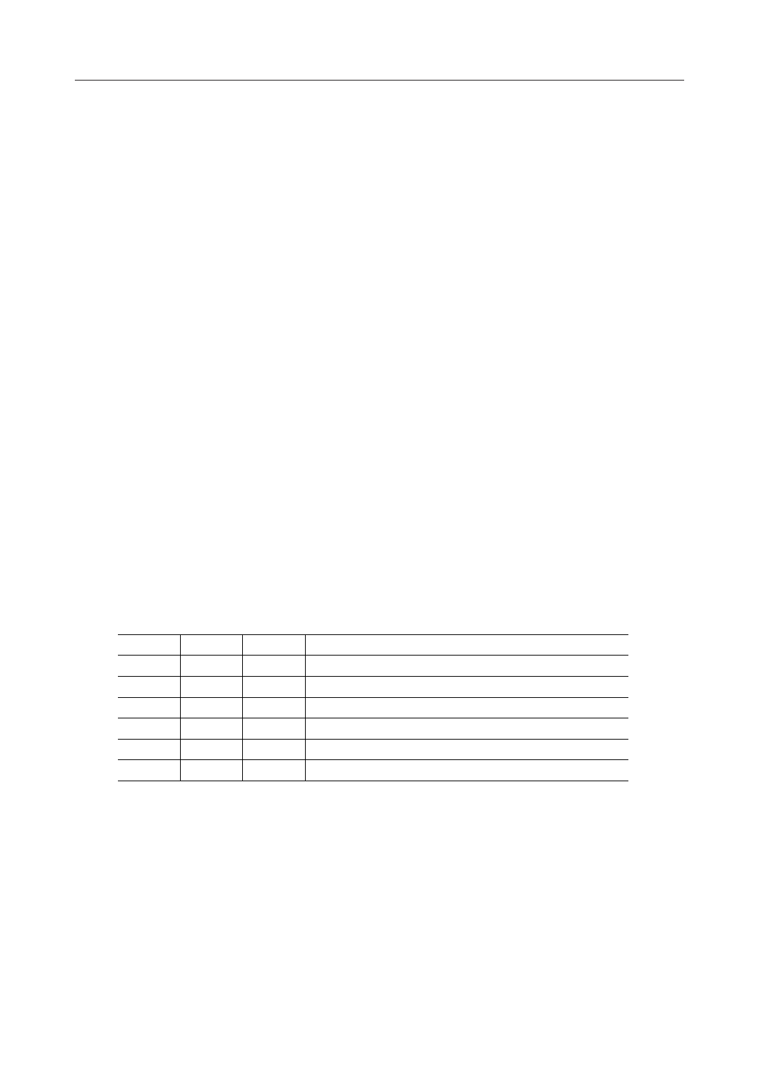
Table 1 Register and R/W pins function table
R/W
RS0
RS1
Function
L
L
H
IR write
H
L
H
Read of busy flag (BF) and address counter (ADC)
L
H
H
DR write
H
H
H
DR read
L
L
L
CR write
H
L
L
CR read
2. Busy Flag (BF)
When the busy flag output is at "H", it indicates that the MSM6562B-xx is engaged in internal
operation.
When the busy flag is at "H" level, any new instruction is ignored.
When R/W = "H", RS0 = "L", and RS1 = "H", the busy flag is output from DB7.
New instruction should be input when BF is "L" level.
When the busy flag is set to "H", the output code of the address counter (ADC) are undefined.
12/50
Share Link: 