MTW32N25E 데이터 시트보기 (PDF) - Motorola => Freescale
부품명
상세내역
제조사
MTW32N25E Datasheet PDF : 8 Pages
| |||
MTW32N25E
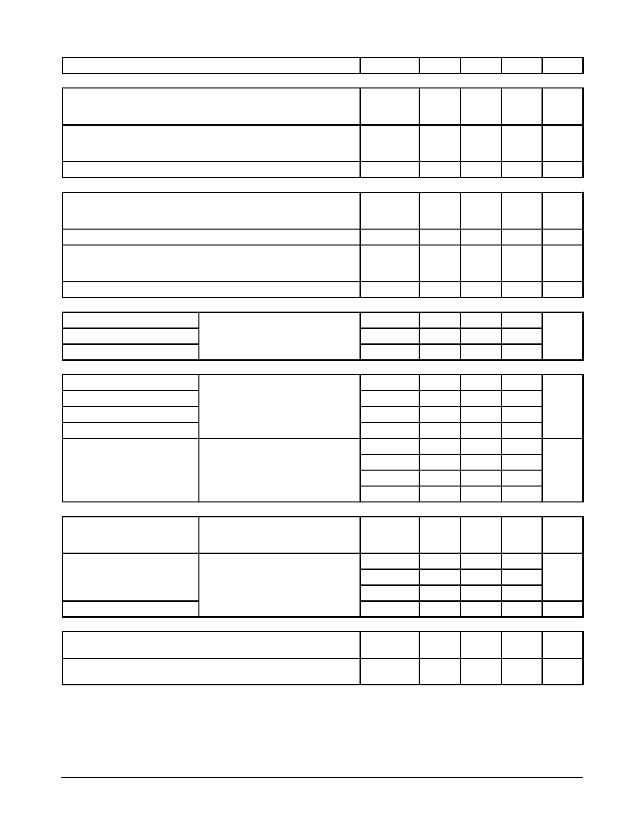
ELECTRICAL CHARACTERISTICS (TJ = 25°C unless otherwise noted)
Characteristic
Symbol
Min
Typ
Max
Unit
OFF CHARACTERISTICS
Drain–Source Breakdown Voltage
(VGS = 0 Vdc, ID = 250 µAdc)
Temperature Coefficient (Positive)
V(BR)DSS
250
300
—
380
—
Vdc
—
mV/°C
Zero Gate Voltage Drain Current
(VDS = 250 Vdc, VGS = 0 Vdc)
(VDS = 250 Vdc, VGS = 0 Vdc, TJ = 125°C)
Gate–Body Leakage Current (VGS = ± 20 Vdc, VDS = 0)
ON CHARACTERISTICS (1)
Gate Threshold Voltage
(VDS = VGS, ID = 250 µAdc)
Temperature Coefficient (Negative)
IDSS
IGSS
µAdc
—
—
10
—
—
100
—
—
100
nAdc
VGS(th)
Vdc
2.0
—
4.0
—
7.0
—
mV/°C
Static Drain–Source On–Resistance (VGS = 10 Vdc, ID = 16 Adc)
Drain–Source On–Voltage (VGS = 10 Vdc)
(ID = 32 Adc)
(ID = 16 Adc, TJ = 125°C)
Forward Transconductance (VDS = 15 Vdc, ID = 16 Adc)
DYNAMIC CHARACTERISTICS
Input Capacitance
Output Capacitance
Reverse Transfer Capacitance
(VDS = 25 Vdc, VGS = 0 Vdc,
f = 1.0 MHz)
SWITCHING CHARACTERISTICS (2)
Turn–On Delay Time
Rise Time
Turn–Off Delay Time
Fall Time
(VDD= 125 Vdc, ID = 32 Adc,
VGS = 10 Vdc,
RG = 9.1 Ω)
Gate Charge
(See Figure 8)
(VDS = 200 Vdc, ID = 32 Adc,
VGS = 10 Vdc)
SOURCE–DRAIN DIODE CHARACTERISTICS
Forward On–Voltage (1)
(IS = 32 Adc, VGS = 0 Vdc)
(IS = 32 Adc, VGS = 0 Vdc, TJ = 125°C)
RDS(on)
VDS(on)
gFS
Ciss
Coss
Crss
td(on)
tr
td(off)
tf
QT
Q1
Q2
Q3
VSD
—
0.07
0.08
Ohm
Vdc
—
2.2
2.6
—
—
2.5
11
20
—
mhos
—
3800
5350
pF
—
726
1020
—
183
370
—
31
60
ns
—
133
266
—
93
186
—
108
216
—
97
136
nC
—
22
—
—
43
—
—
41
—
Vdc
—
1.0
1.5
—
0.92
—
Reverse Recovery Time
(See Figure 14)
(IS = 32 Adc, VGS = 0 Vdc,
dIS/dt = 100 A/µs)
Reverse Recovery Stored Charge
INTERNAL PACKAGE INDUCTANCE
Internal Drain Inductance
(Measured from the drain lead 0.25″ from package to center of die)
trr
ta
tb
QRR
LD
—
312
—
ns
—
220
—
—
93
—
—
3.6
—
µC
—
4.5
—
nH
Internal Source Inductance
LS
(Measured from the source lead 0.25″ from package to source bond pad)
—
13
—
nH
(1) Pulse Test: Pulse Width ≤ 300 µs, Duty Cycle ≤ 2%.
(2) Switching characteristics are independent of operating junction temperature.
2
Motorola TMOS Power MOSFET Transistor Device Data
Share Link: 