NCP4680 데이터 시트보기 (PDF) - ON Semiconductor
부품명
상세내역
제조사
NCP4680 Datasheet PDF : 20 Pages
| |||
NCP4680
APPLICATION INFORMATION
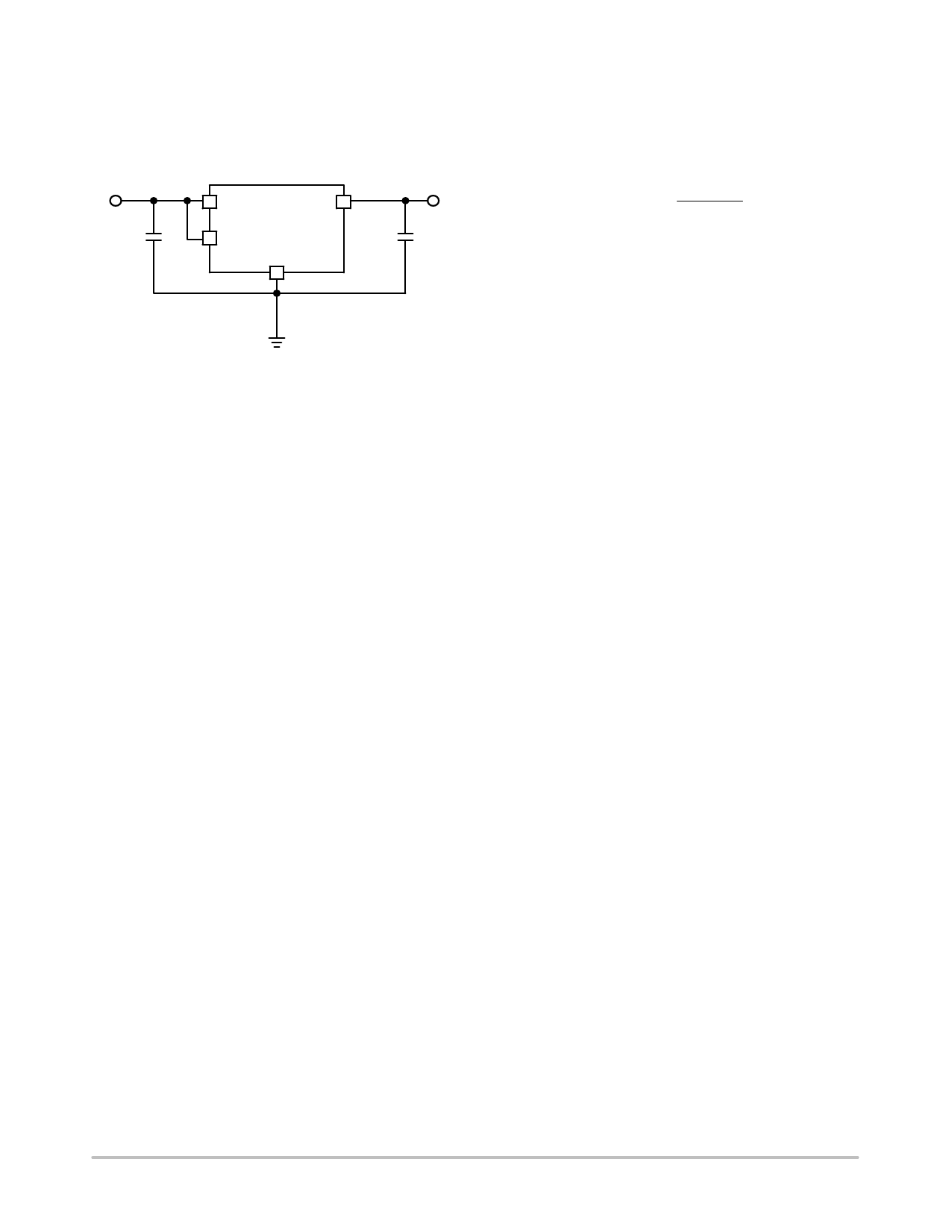
A typical application circuit for NCP4680 series is shown
in Figure 55.
VIN
NCP4680x
VOUT
VIN
VOUT
C1
100n
CE
GND
C2
100n
start−up into at least double the minimum equivalent load.
The minimum equivalent resistance can be computed by
formula 1:
VOUT(NOM)
REQMIN + IOUTMAX
(eq. 1)
This leads us to the result that the minimum equivalent
start up resistance for VOUT(NOM) < 1.8 V is:
RSUMIN + 2 @ REQMIN
(eq. 2)
Figure 55. Typical Application Schematic
Input Decoupling Capacitor (C1)
A 0.1 mF ceramic input decoupling capacitor should be
connected as close as possible to the input and ground pin of
the NCP4680. Higher values and lower ESR improves line
transient response.
Output Decoupling Capacitor (C2)
A 0.1 mF ceramic output decoupling capacitor is enough
to achieve stable operation of the IC. If a tantalum capacitor
is used, and its ESR is high, loop oscillation may result. The
capacitors should be connected as close as possible to the
output and ground pins. Larger values and lower ESR
improves dynamic parameters.
Current Limit
The NCP4680 includes fold−back type current limit
protection. Its typical characteristic for 0.8 V version is
shown in Figure 3. The advantage of this protection is that
power loss at the regulator is minimized at over current or
short circuit conditions. When the over current or short
circuit event disappears, the regulator reverts from fold back
to regulation. This kind of current limit may cause issues at
start−up for voltage versions below 1.8 V and some load
types: for these lower voltage options it is recommended to
Enable Operation
The enable pin CE may be used for turning the regulator
on and off. The IC is switched on when a high level voltage
is applied to the CE pin. The enable pin has an internal pull
down current source. If the enable function is not needed
connect CE pin to VIN.
Output Discharger
The D version includes a transistor between VOUT and
GND that is used for faster discharging of the output
capacitor. This function is activated when the IC goes into
disable mode.
Thermal
As power across the IC increase, it might become
necessary to provide some thermal relief. The maximum
power dissipation supported by the device is dependent
upon board design and layout. Mounting pad configuration
on the PCB, the board material, and also the ambient
temperature affect the rate of temperature increase for the
part. When the device has good thermal conductivity
through the PCB the junction temperature will be relatively
low in high power dissipation applications.
PCB layout
Make the VIN and GND line as large as practical. If their
impedance is high, noise pickup or unstable operation may
result. Connect capacitors C1 and C2 as close as possible to
the IC, and make wiring as short as possible.
http://onsemi.com
16
Share Link: 