P89C51X2 데이터 시트보기 (PDF) - Philips Electronics
부품명
상세내역
제조사
P89C51X2 Datasheet PDF : 48 Pages
| |||

Philips Semiconductors
80C51 8-bit Flash microcontroller family
4K/8K/16K/32K Flash
Preliminary data
P89C51X2/52X2/54X2/58X2
Power-Down Mode
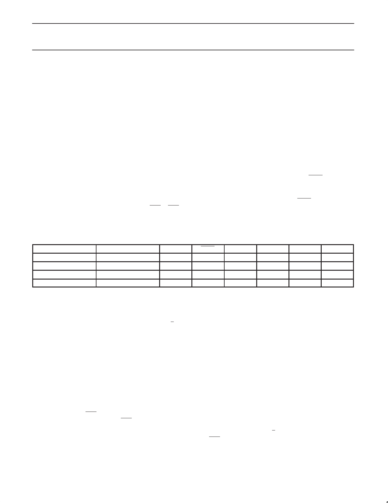
To save even more power, a Power Down mode (see Table 3) can
be invoked by software. In this mode, the oscillator is stopped and
the instruction that invoked Power Down is the last instruction
executed. The on-chip RAM and Special Function Registers retain
their values down to 2.0 V and care must be taken to return VCC to
the minimum specified operating voltages before the Power Down
Mode is terminated.
Either a hardware reset or external interrupt can be used to exit from
Power Down. Reset redefines all the SFRs but does not change the
on-chip RAM. An external interrupt allows both the SFRs and the
on-chip RAM to retain their values. WUPD (AUXR1.3–Wakeup from
Power Down) enables or disables the wakeup from power down with
external interrupt. Where:
WUPD = 0: Disable
WUPD = 1: Enable
To properly terminate Power Down, the reset or external interrupt
should not be executed before VCC is restored to its normal
operating level and must be held active long enough for the
oscillator to restart and stabilize (normally less than 10 ms).
To terminate Power Down with an external interrupt, INT0 or INT1
must be enabled and configured as level-sensitive. Holding the pin
low restarts the oscillator but bringing the pin back high completes
the exit. Once the interrupt is serviced, the next instruction to be
executed after RETI will be the one following the instruction that put
the device into Power Down.
Design Consideration
When the idle mode is terminated by a hardware reset, the device
normally resumes program execution from where it left off, up to two
machine cycles before the internal reset algorithm takes control.
On-chip hardware inhibits access to internal RAM in this event, but
access to the port pins is not inhibited. To eliminate the possibility of
an unexpected write when Idle is terminated by reset, the instruction
following the one that invokes Idle should not be one that writes to a
port pin or to external memory.
ONCE™ Mode
The ONCE (“On-Circuit Emulation”) Mode facilitates testing and
debugging of systems without the device having to be removed from
the circuit. The ONCE Mode is invoked in the following way:
1. Pull ALE low while the device is in reset and PSEN is high;
2. Hold ALE low as RST is deactivated.
While the device is in ONCE Mode, the Port 0 pins go into a float
state, and the other port pins and ALE and PSEN are weakly pulled
high. The oscillator circuit remains active. While the device is in this
mode, an emulator or test CPU can be used to drive the circuit.
Normal operation is restored when a normal reset is applied.
Table 3. External Pin Status During Idle and Power-Down Modes
MODE
PROGRAM MEMORY
ALE
PSEN
PORT 0
Idle
Internal
1
1
Data
Idle
External
1
1
Float
Power-down
Internal
0
0
Data
Power-down
External
0
0
Float
PORT 1
Data
Data
Data
Data
PORT 2
Data
Address
Data
Data
PORT 3
Data
Data
Data
Data
TIMER 0 AND TIMER 1 OPERATION
Timer 0 and Timer 1
The “Timer” or “Counter” function is selected by control bits C/T in
the Special Function Register TMOD. These two Timer/Counters
have four operating modes, which are selected by bit-pairs (M1, M0)
in TMOD. Modes 0, 1, and 2 are the same for both Timers/Counters.
Mode 3 is different. The four operating modes are described in the
following text.
Mode 0
Putting either Timer into Mode 0 makes it look like an 8048 Timer,
which is an 8-bit Counter with a divide-by-32 prescaler. Figure 2
shows the Mode 0 operation.
In this mode, the Timer register is configured as a 13-bit register. As
the count rolls over from all 1s to all 0s, it sets the Timer interrupt
flag TFn. The counted input is enabled to the Timer when TRn = 1
and either GATE = 0 or INTn = 1. (Setting GATE = 1 allows the
Timer to be controlled by external input INTn, to facilitate pulse width
measurements). TRn is a control bit in the Special Function Register
TCON (Figure 3).
The 13-bit register consists of all 8 bits of THn and the lower 5 bits
of TLn. The upper 3 bits of TLn are indeterminate and should be
ignored. Setting the run flag (TRn) does not clear the registers.
Mode 0 operation is the same for Timer 0 as for Timer 1. There are
two different GATE bits, one for Timer 1 (TMOD.7) and one for Timer
0 (TMOD.3).
Mode 1
Mode 1 is the same as Mode 0, except that the Timer register is
being run with all 16 bits.
Mode 2
Mode 2 configures the Timer register as an 8-bit Counter (TLn) with
automatic reload, as shown in Figure 4. Overflow from TLn not only
sets TFn, but also reloads TLn with the contents of THn, which is
preset by software. The reload leaves THn unchanged.
Mode 2 operation is the same for Timer 0 as for Timer 1.
Mode 3
Timer 1 in Mode 3 simply holds its count. The effect is the same as
setting TR1 = 0.
Timer 0 in Mode 3 establishes TL0 and TH0 as two separate
counters. The logic for Mode 3 on Timer 0 is shown in Figure 5. TL0
uses the Timer 0 control bits: C/T, GATE, TR0, and TF0 as well as
pin INT0. TH0 is locked into a timer function (counting machine
cycles) and takes over the use of TR1 and TF1 from Timer 1. Thus,
TH0 now controls the “Timer 1” interrupt.
2002 Jun 06
12