R1LV0408CSA 데이터 시트보기 (PDF) - Renesas Electronics
부품명
상세내역
제조사
R1LV0408CSA Datasheet PDF : 14 Pages
| |||
R1LV0408C-I Series
Low VCC Data Retention Characteristics
(Ta = −40 to +85°C)
Parameter
Symbol Min Typ Max Unit Test conditions*3
VCC for data retention
VDR
2.0 V CS# ≥ VCC − 0.2 V, Vin ≥ 0 V
Data
retention
current
−5SI
to +85°C
to +70°C
to +40°C
to +25°C
ICCDR
ICCDR
ICCDR
ICCDR
10 µA VCC = 3.0 V, Vin ≥ 0 V
8
0.7*2 3
µA CS# ≥ VCC − 0.2 V
µA
0.5*1 3 µA
−7LI
to +85°C
ICCDR
20 µA
to +70°C
to +40°C
to +25°C
ICCDR
ICCDR
ICCDR
16 µA
0.7*2 10 µA
0.5*1 10 µA
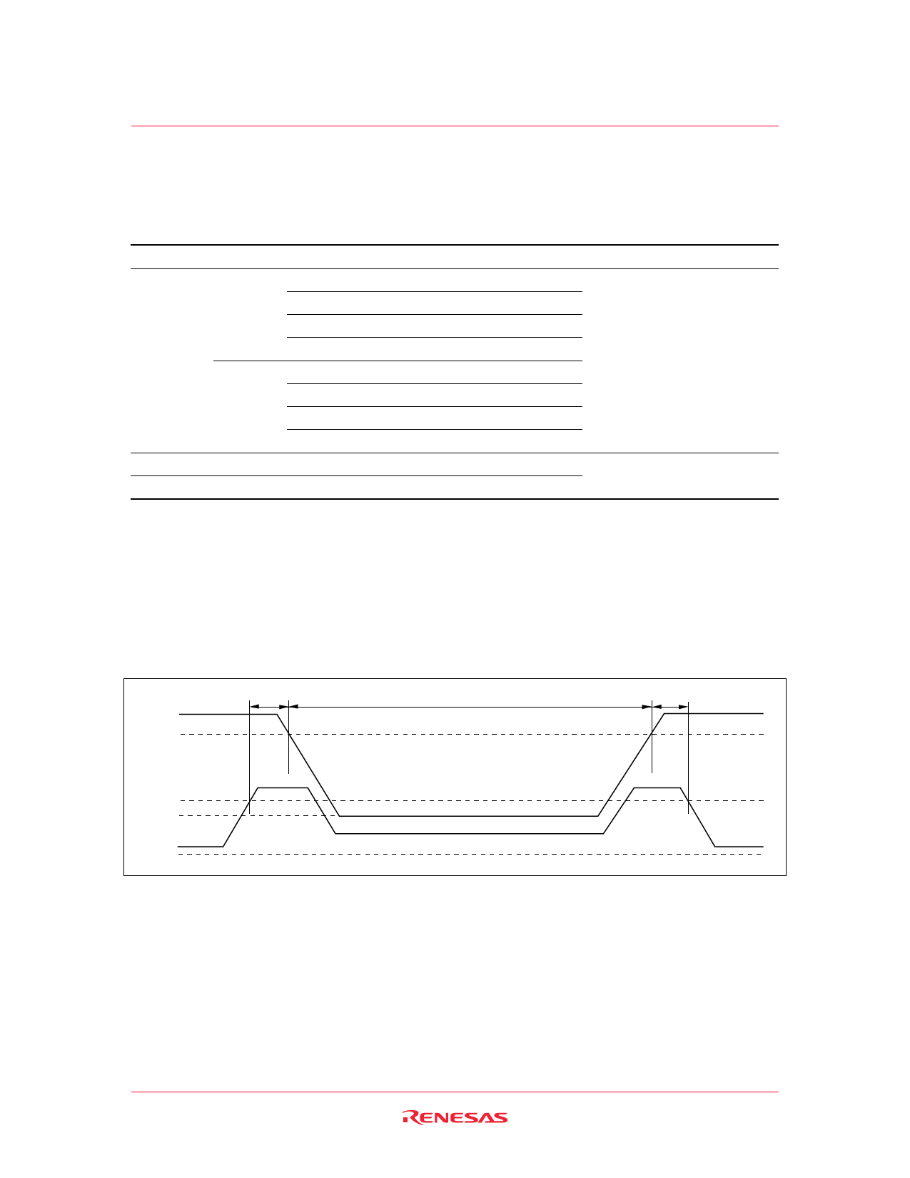
Chip deselect to data retention time
tCDR
Operation recovery time
tR
0
tRC*4
ns See retention waveform
ns
Notes: 1. Typical values are at VCC = 3.0 V, Ta = +25°C and specified loading, and not guaranteed.
2. Typical values are at VCC = 3.0 V, Ta = +40°C and specified loading, and not guaranteed.
3. CS# controls address buffer, WE# buffer, OE# buffer, and Din buffer. In data retention mode,
Vin levels (address, WE#, OE#, I/O) can be in the high impedance state.
4. tRC = read cycle time.
Low VCC Data Retention Timing Waveform (CS# Controlled)
tCDR
Data retention mode
tR
VCC
2.7 V
2.2 V
VDR
CS#
0V
CS# ≥ VCC – 0.2 V
Rev.2.00, May.25.2004, page 12 of 12
Share Link: 