RF3159 데이터 시트보기 (PDF) - RF Micro Devices
부품명
상세내역
제조사
RF3159 Datasheet PDF : 26 Pages
| |||
RF3159
GSM (Saturated) Mode
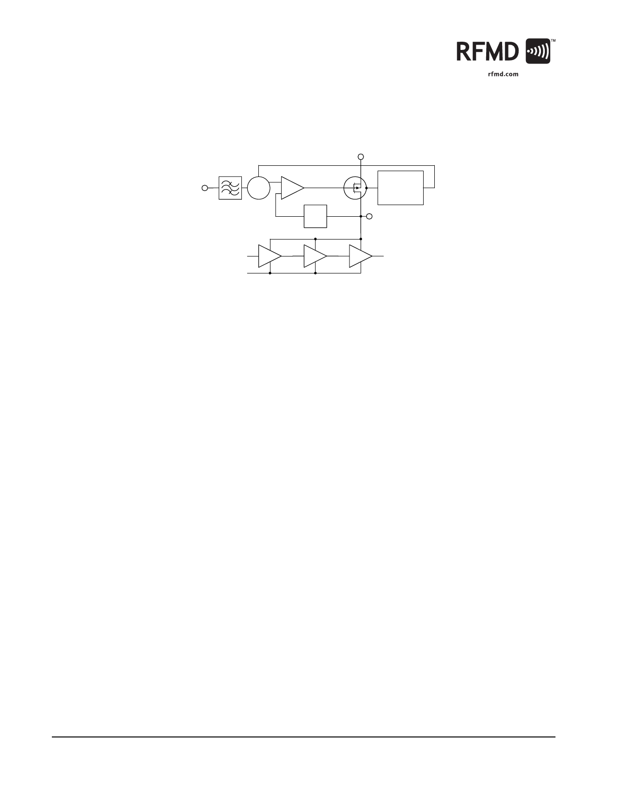
In GSM mode, RF3159 operates as a traditional PowerStar® module. The incorporated control loop regulates the collector volt-
age of the amplifiers while the stages are held at a constant bias. The basic circuit diagram is shown in Figure 2.
VBATT
3 dB BW
300 kHz
VRAMP
--
+
+
Saturation
Detector
H(s)
VCC
RF IN
TX ENABLE
Figure 2. RF3159 Basic Circuit Diagram
RF OUT
By regulating the collector voltage (VCC), the stages are held in saturation across all power levels. As VCC is decreased, output
power decreases as described by Equation 1. The equation shows that load impedance affects output power, but to a lesser
degree than VCC supply variations. Since the RF3159 regulates VCC, the dominant cause of power variation is eliminated.
POUTdBm
=
10log -(--2----⋅---V----C----C----–-----V----S---A---T---)--2- (Eq. 1)
8 ⋅ R1 ⋅ 10–3
RF3159 power is ramped up and down through the VRAMP control voltage which in turn controls the collector voltage of the
amplifier stages. The RF signal applied at the RFIN pin must be a constant amplitude signal and should be high enough to sat-
urate the amplifier in the GSM mode. The input power (PIN) range is indicated in the specifications. Power levels below this
range will result in reduced maximum output power and the potential for more variation of output power over extreme condi-
tions. Higher input power is unnecessary and will require more current in the circuitry driving the power amplifier and will
increase the minimum output power of the RF3159.
The saturation detector circuit monitors the VBATT and VCC voltages and adjusts the power control loop to prevent the series-
pass FET regulator from entering saturation. If the VCC regulator were to saturate, the response time would increase dramati-
cally. This is undesirable because the VCC regulator must accurately follow the burst ramp up or ramp down applied to the
VRAMP pin, or the transient spectrum will degrade.
EDGE (Linear) Mode
In EDGE mode, VCC is fixed and one of two preset bias ranges is selectable by the VBIAS pin. EDGE mode gain is reduced from
GSM mode by switchable attenuators and the RF3159 operates as a linear amplifier where output power is directly controlled
by input power. The RF signal applied to the RFIN pin must be accurately controlled to produce the desired output amplitude
and burst ramping. The RFIN power must be maintained so that the amplifier is operating in its linear region. If the input drive
is too high, the amplifier will begin to saturate causing the ACPR and EVM performance to degrade. The most sensitive of these
on the RF3159 is the +/-400kHz offset ACPR. As the amplifier approaches saturation, this will be the first parameter to show
significant degradation.
During production calibration of a system containing the RF3159, the PA gain and other parameters must be determined. After
that, the RF3159 functions as a fixed gain block while the system adjusts input power such that the output from the transmit-
ter meets the desired system specifications.
18 of 26
7628 Thorndike Road, Greensboro, NC 27409-9421 · For sales or technical
support, contact RFMD at (+1) 336-678-5570 or sales-support@rfmd.com.
Rev A0 DS070102
Share Link: 