RS5C316 데이터 시트보기 (PDF) - RICOH Co.,Ltd.
부품명
상세내역
제조사
RS5C316 Datasheet PDF : 38 Pages
| |||
RS5C316A/B
2. Write Data (For the RS5C316A)
Writing data to the real-time clock requires inputting setting data (control bits, address bits and data bits) to the
SIO pin and then establishing the write mode by using a control bit R/W in the same manner as in read operation.
*) Control bits and address bits are described in the previous section on read cycle.
• Data bits
D3-D0: Inputs the data bits MSB to LSB in the addressing table describing the functions.
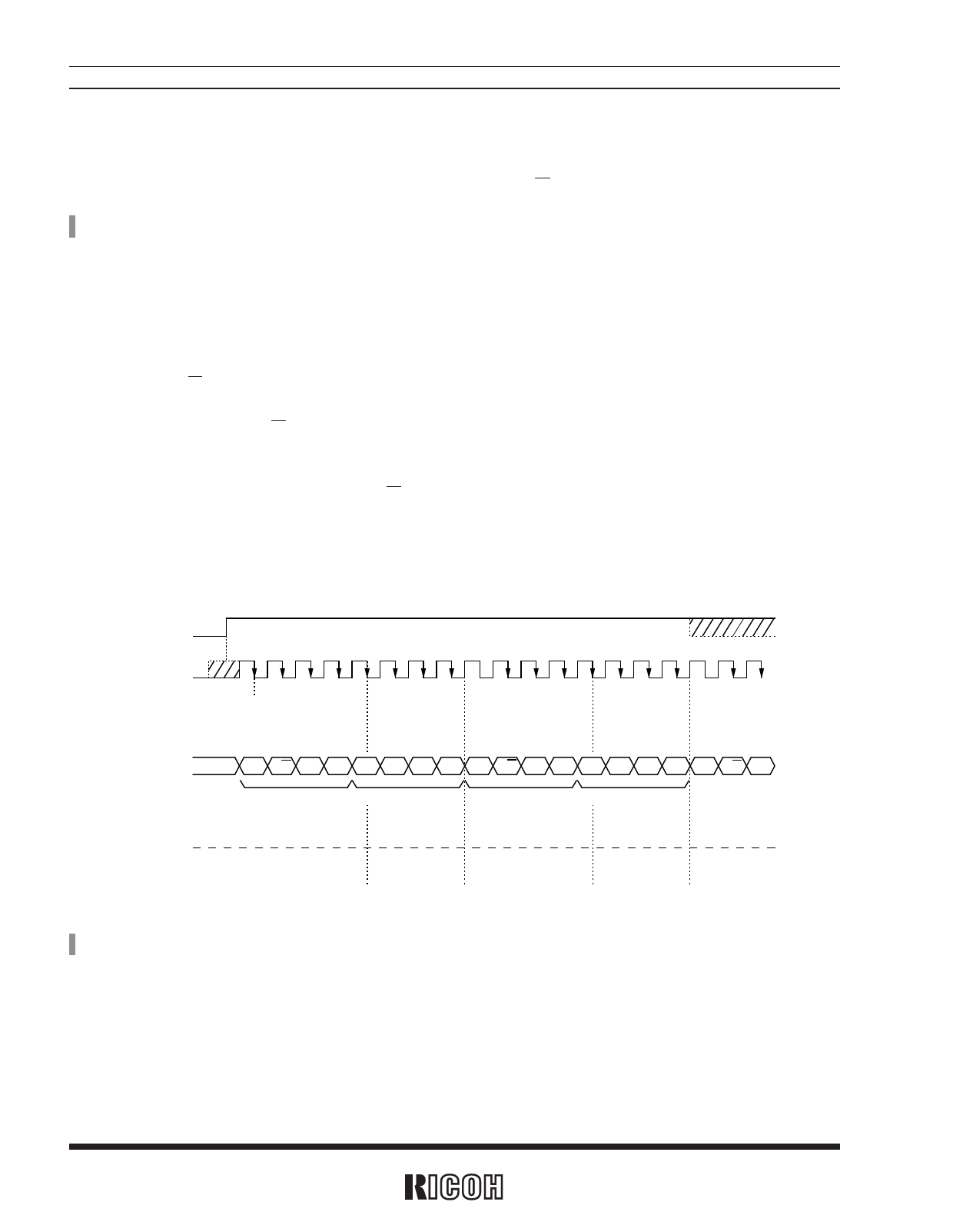
2.1 Write Cycle Flow
1. The CE pin is switched from “L” to “H”.
2. Four control bits (with the first bit ignored) and four write address bits are input from the SIO pin. At this time,
control bits R/W and DT are set equally to 0 while a control bit AD is set to 1. (see the SCLK 1A-8A)
3. Four control bits and four bits of data to be written are input in the descending order of their significance.
At this time, control bits R/W and AD are set equally to 0 while a control bit DT is set to 1. (see the clock 1B-8B)
4. When write cycle is continued, control bits and address bits are input at the shift clock pulse 1C and later in the
same manner as at the shift clock pulse 1A.
5. At the end of write operation, control bits R/W, AD, and DT are set equally to 0 (at the falling edge of shift clock
pulse 5A and later from the SCLK pin) or the CE pin is switched from “H” to “L” (after tCEH from the falling edge
of the eighth shift clock pulse from the SCLK pin). Following on write cycle, read operation can be performed by
setting control bits in the read mode at the shift clock pulse 1C and later with the CE pin held at “H”.
CE
SCLK
1A 2A 3A 4A 5A 6A 7A 8A 1B 2B 3B 4B 5B 6B 7B 8B 1C 2C 3C
Input to
SIO pin
Writing to shift
register
*
* R/W AD DT A3 A2 A1 A0 * R/W AD DT D3 D2 D1 D0 * R/W AD
Control bits
Address bits Control bits
Data bits
Output
from
SIO pin
(Hiz)
(Internal processing)
Setting of
control bits
Writing to address
register
Setting of
control bits
(Hiz)
End of write
operation
* * ) In the above figure, the “ ” mark indicates arbitrary data; and the diagonally shaded area of CE and SCLK indicates “H” or “L”.
16
Share Link: 