RV4141A 데이터 시트보기 (PDF) - Fairchild Semiconductor
부품명
상세내역
제조사
RV4141A Datasheet PDF : 9 Pages
| |||
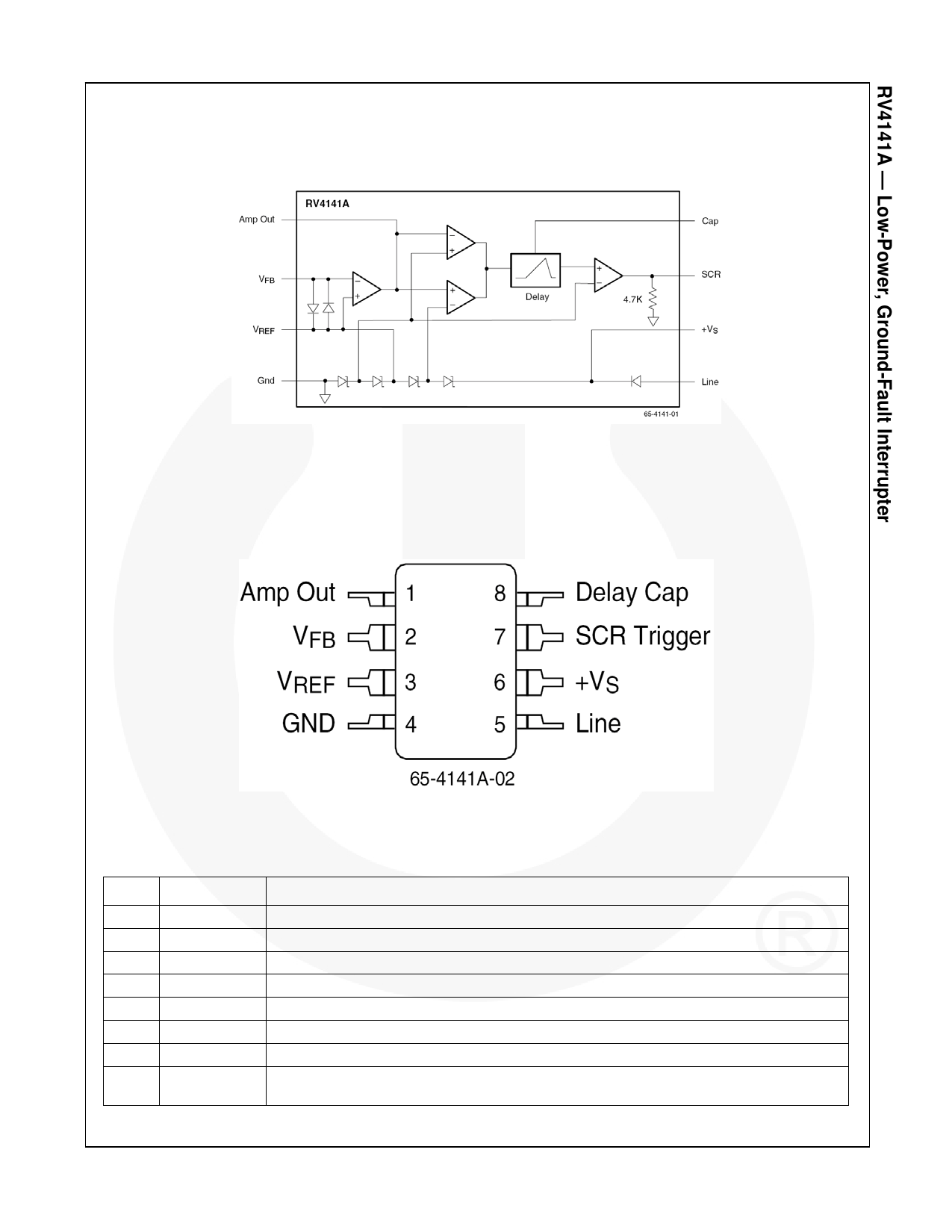
Block Diagram
Pin Configuration
Figure 1. Block Diagram
Figure 2. Pin Assignment
Pin Definitions
Pin #
1
2
3
4
5
6
7
8
Name
Amp Out
VFB
VREF
GND
Line
+VS
SCR Trigger
Delay Cap
Description
Sense Amplifier Output – an external resistor to VFB sets the IFAULT threshold
Sense amplifier negative input
Sense amplifier positive input – biased internally at +VS/2
Substrate ground for all circuitry
Anode of internal diode connected to supply voltage
Supply input for RV4141A circuitry
Output for triggering external SCR when a fault is detected
An external capacitor to ground sets the delay time for a ground fault to be present before
triggering the SCR
© 2003 Fairchild Semiconductor Corporation
RV4141A • Rev. 1.0.8
2
www.fairchildsemi.com
Share Link: 