S-1112A39MC-L6YTFG 데이터 시트보기 (PDF) - Unspecified
부품명
상세내역
제조사
S-1112A39MC-L6YTFG Datasheet PDF : 31 Pages
| |||
HIGH RIPPLE-REJECTION AND LOW DROPOUT CMOS VOLTAGE REGULATOR
S-1112/1122 Series
Rev.6.1_02
Operation
1. Basic operation
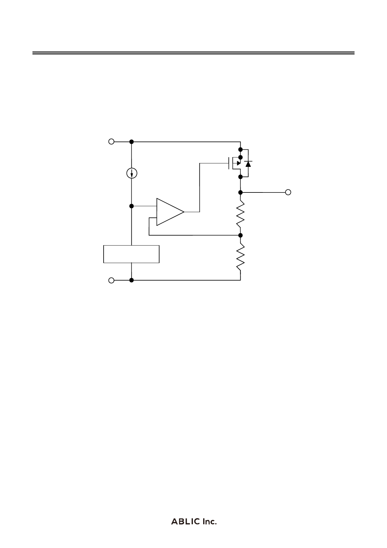
Figure 12 shows the block diagram of the S-1112/1122 Series.
The error amplifier compares the reference voltage (Vref) with feedback voltage (Vfb), which is the output
voltage resistance-divided by feedback resistors (Rs and Rf). It supplies the gate voltage necessary to
maintain the constant output voltage which is not influenced by the input voltage and temperature
change, to the output transistor.
VIN
Current
supply
Vref
Error
amplifier
Reference voltage
circuit
*1
Rf
Vfb
Rs
VOUT
VSS
*1. Parasitic diode
Figure 12
2. Output transistor
In the S-1112/1122 Series, a low on-resistance P-channel MOS FET is used as the output transistor.
Be sure that VOUT does not exceed VIN 0.3 V to prevent the voltage regulator from being damaged due
to reverse current flowing from the VOUT pin through a parasitic diode to the VIN pin, when the potential
of VOUT became higher than VIN.
14
Share Link: 