Q65110A6458(2015) 데이터 시트보기 (PDF) - OSRAM GmbH
부품명
상세내역
제조사
Q65110A6458 Datasheet PDF : 13 Pages
| |||
Version 1.2 (not for new design in automotive applications)
SFH 3010
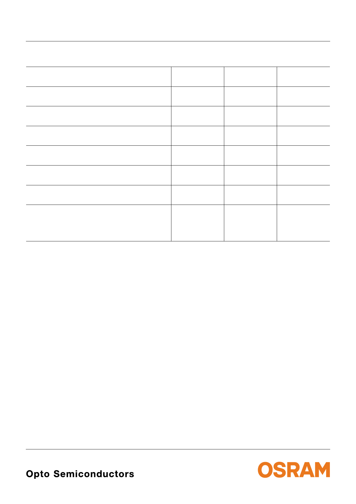
Maximum Ratings (TA = 25 °C)
Parameter
Operating and storage temperature range
Collector-emitter voltage
Collector-emitter voltage
(t < 2 min)
Collector current
Collector surge current
(τ < 10 µs)
Emitter-collector voltage
Total Power dissipation
Electrostatic discharge
(acc. to ANSI/ ESDA/ JEDEC JS-001 - HBM)
Thermal resistance for mounting on pcb
Thermal restistance junction 1) page 12
Characteristics (TA = 25 °C)
Parameter
Wavelength of max. sensitivity
Spectral range of sensitivity
Radiant sensitive area
Dimensions of chip area
Half angle
Capacitance
(VCE = 0 V, f = 1 MHz, E = 0)
Photocurrent
(λ = 950 nm, Ee = 0.5 mW/cm2, VCE = 5 V)
Dark current
(VCE = 20 V, E = 0)
Rise and fall time
(IC = 1 mA, VCC = 5 V, RL = 1 kΩ)
Collector-emitter saturation voltage
(IC = 10 μA, Ee = 0.5 mW/cm2, λ = 950 nm, )
Symbol
Top; Tstg
VCE
VCE
IC
ICS
VEC
Ptot
VESD
RthJA
RthJS
Values
-40 ... 100
15
30
15
75
7
130
2000
450
250
Unit
°C
V
V
mA
mA
V
mW
V
K/W
K/W
(typ)
(typ)
(typ)
(typ)
Symbol
λS max
λ10%
A
LxW
(typ)
ϕ
(typ)
CCE
IPCE
(typ (max)) ICE0
(typ)
tr, tf
(typ)
VCEsat
Values
Unit
860
nm
(typ) 420
... 1100
0.04
nm
mm2
(typ) 0.38 x mm x
0.38
mm
± 80
°
1.3
pF
≥ 25
µA
1 (≤ 50)
nA
7
µs
140
mV
2015-12-08
2
Share Link: 