M80C186 데이터 시트보기 (PDF) - Intel
부품명
상세내역
제조사
M80C186 Datasheet PDF : 59 Pages
| |||
M80C186
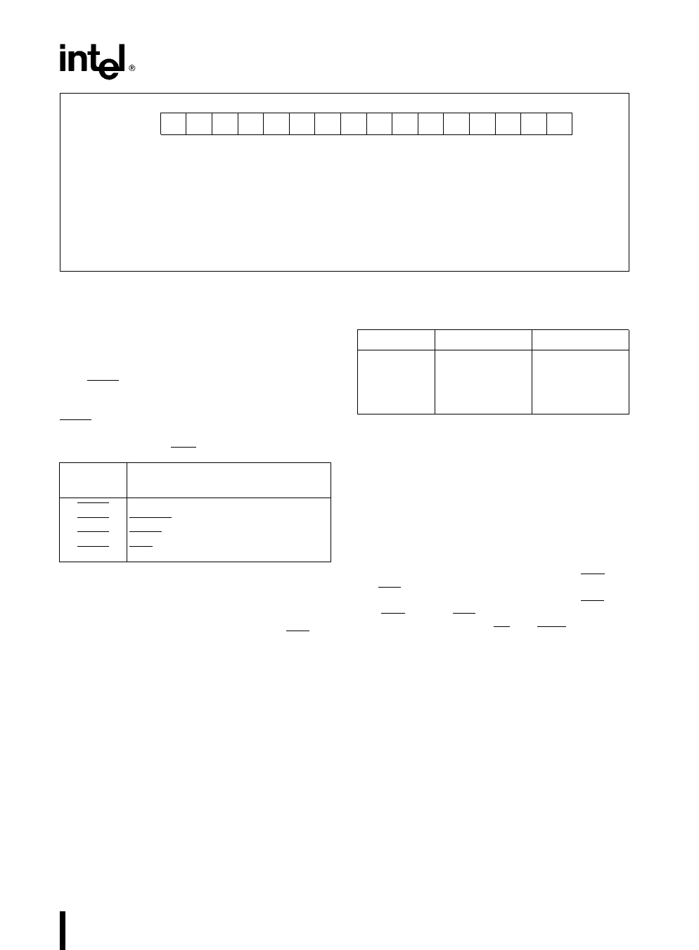
15 14 13 12 11 10 9 8 7 6 5 4 3 2 1 0
PDCON
E 0 0 0 0 0 0 0 0 0 0 0 0 0 F1 F0
Offset F0H
Bits 0–1
Bits 2–14
Bit 15
Clock Divisor Select
F1 F0 Division Factor
0
0 divide by 1
0
1 divide by 4
1
0 divide by 8
1
1 divide by 16
Reserved read back as zero
Enable Power Save Mode Set to zero on RESET
Figure 44 Power-Save Control Register
Numeric Coprocessor (NPX)
Extension
Three of the mid-range memory chip selects are re-
defined according to Table 16 when using the nu-
merics coprocessor extension The fourth chip se-
lect MCS2 functions as in compatible mode and
may be programmed for activity with ready logic and
wait states accordingly As in compatible mode
MCS2 will function for one-fourth a programmed
block size
Table 16 MCS Assignments
Compatible
Mode
Enhanced Mode
MCS0
MCS1
MCS2
MCS3
PEREQ Processor Extension Request
ERROR NPX Error
MCS2 Mid-Range Chip Select
NPS Numeric Processor Select
Table 17 Numerics Coprocessor I O Port
Assignments
I O Address Read Definition Write Definition
00F8H
00FAH
00FCH
00FEH
Status Control
Data
reserved
Opcode Status
Opcode
Data
CS IP DS EA
reserved
‘‘ONCE’’ Test Mode
To facilitate testing and inspection of devices when
fixed into a target system the M80C186 has a test
mode available which allows all pins to be placed in
a high-impedance state ‘‘ONCE’’ stands for ‘‘ON
Circuit Emulation’’ When placed in this mode the
M80C186 will put all pins in the high-impedance
state until RESET
Four port addresses are assigned to the NPX for 16-
bit reads and writes by the M80C186 Table 17
shows the port definitions These ports are not ac-
cessible by using the M80C186 I O instructions
However numerics operations will cause a PCS line
to be activated if it is properly programmed for this
I O range
The ONCE mode is selected by tying the UCS and
the LCS LOW during RESET These pins are sam-
pled on the low-to-high transition of the RES pin
The UCS and the LCS pins have weak internal pull-
up resistors similar to the RD and TEST BUSY pins
to guarantee proper normal operation
43
Share Link: 