80C251TA 데이터 시트보기 (PDF) - Intel
부품명
상세내역
제조사
80C251TA Datasheet PDF : 34 Pages
| |||
8xC251TA/TB/TP/TQ HIGH-PERFORMANCE CHMOS MICROCONTROLLER
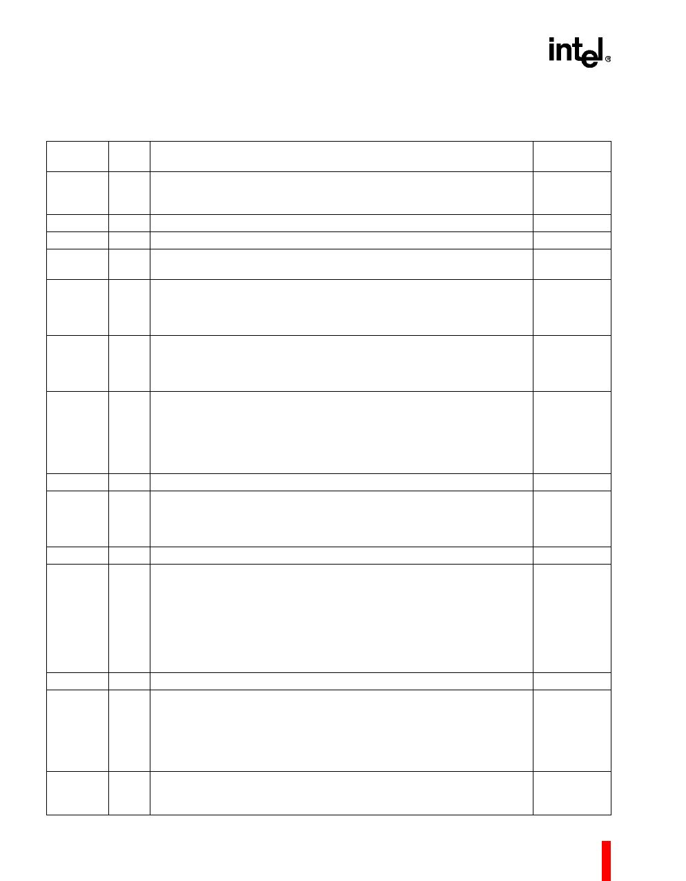
4.0 SIGNALS
Signal
Name
A17
A16
A15:81
AD7:01
ALE
CEX4:0
EA#
ECI
INT1:0#
P0.7:0
P1.0
P1.1
P1.2
P1.7:3
P2.7:0
P3.0
P3.1
P3.3:2
P3.5:4
P3.6
P3.7
PSEN#
Table 6. Signal Descriptions (Sheet 1 of 3)
Type
O
O
O
I/O
O
I/O
I
I
I
I/O
I/O
I/O
I/O
O
Description
18th Address Bit (A17). Output to memory as 18th external address bit
(A17) in extended bus applications, depending on the values of bits RD0
and RD1 in configuration byte UCONFIG0. See also RD# and PSEN#.
Address Line 16. See RD#.
Address Lines. Upper address lines for the external bus.
Address/Data Lines. Multiplexed lower address lines and data lines for
external memory.
Address Latch Enable. ALE signals the start of an external bus cycle
and indicates that valid address information is available on lines A15:8
and AD7:0. An external latch can use ALE to demultiplex the address
from the address/data bus.
Programmable Counter Array (PCA) Input/Output Pins. These are
input signals for the PCA capture mode and output signals for the PCA
compare mode and PCA PWM mode.
External Access. Directs program memory accesses to on-chip or off-
chip code memory. For EA# = 0, all program memory accesses are off-
chip. For EA# = 1, an access is to on-chip ROM if the address is within
the range of the on-chip ROM; otherwise the access is off-chip. The value
of EA# is latched at reset. For devices without on-chip ROM, EA# must
be strapped to ground.
PCA External Clock Input. External clock input to the 16-bit PCA timer.
External Interrupts 0 and 1. These inputs set bits IE1:0 in the TCON
register. If bits IT1:0 in the TCON register are set, bits IE1:0 are set by a
falling edge on INT1#/INT0#. If bits INT1:0 are clear, bits IE1:0 are set by
a low level on INT1:0#.
Port 0. This is an 8-bit, open-drain, bidirectional I/O port.
Port 1. This is an 8-bit, bidirectional I/O port with internal pullups.
Port 2. This is an 8-bit, bidirectional I/O port with internal pullups.
Port 3. This is an 8-bit, bidirectional I/O port with internal pullups.
Program Store Enable. Read signal output. This output is asserted for a
memory address range that depends on bits RD0 and RD1 in configu-
ration byte UCONFIG0 (see RD#).
Alternate
Function
P1.7/CEX4/
WCLK
RD#
P2.7:0
P0.7:0
P1.6:4
P1.7/A17/
WAIT#
P1.3/TXD1
P1.2/RXD1
P3.3:2
AD7:0
T2
T2EX
ECI/RXD1
CEX3:1
CEX4/A17/
WAIT#/
WCLK
CEX0/TXD1
A15:8
RXD
TXD
INT1:0#
T1:0
WR#
RD#/A16
—
8
ADVANCE INFORMATION
Share Link: 