HMS87C4260 데이터 시트보기 (PDF) - Hynix Semiconductor
부품명
상세내역
제조사
HMS87C4260 Datasheet PDF : 110 Pages
| |||
HMS81C4x60
7. ELECTRICAL CHARACTERISTICS
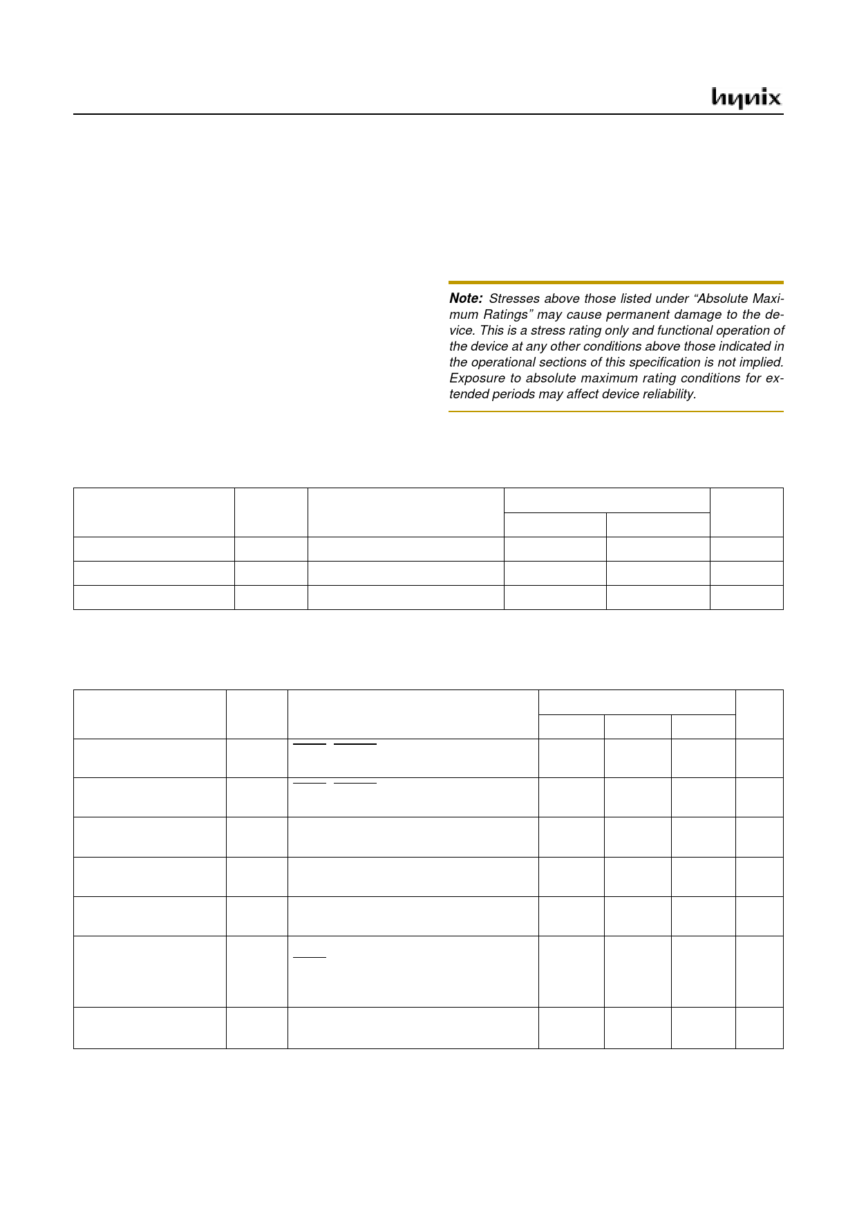
7.1 Absolute Maximum Ratings
Supply voltage ........................................... -0.3 to +6.0 V
Storage Temperature ................................-40 to +125 °C
Voltage on any pin with respect to Ground (VSS)
............................................................... -0.3 to VDD+0.3
Maximum current out of Vss pin.........................160 mA
Maximum current into VDD pin ..........................160 mA
Maximum current sunk by(IOL per I/O Pin) .........20 mA
Maximum output current sourced by (IOH per I/O Pin)
.................................................................................8 mA
7.2 Recommended Operating Conditions
Maximum current (ΣIOL) .................................... 100 mA
Maximum current (ΣIOH)...................................... 80 mA
Note: Stresses above those listed under “Absolute Maxi-
mum Ratings” may cause permanent damage to the de-
vice. This is a stress rating only and functional operation of
the device at any other conditions above those indicated in
the operational sections of this specification is not implied.
Exposure to absolute maximum rating conditions for ex-
tended periods may affect device reliability.
Parameter
Supply Voltage
Operating Frequency
Operating Temperature
Symbol
VDD
fXIN
TOPR
Condition
VDD=4.5~5.5V
fXIN=4MHz
Specifications
Min.
Max.
4.5
5.5
-
4.0(typical)
-10
70
Unit
V
MHz
°C
7.3 DC Electrical Characteristics
(TA=-10~70°C, VDD=4.5~5.5V),
Parameter
Symbol
Condition
High level input voltage
Low level input voltage
High level output voltage
Low level output voltage
Supply current in
ACTIVE mode
pull-up lekage current
High input leakage
current
VIH
VIL
VOH
VOL
IDD
IRUP
IIZH
TEST, RESET, Xin, R0, R1, R2, R3,
HS, VS
TEST, RESET, Xin, R0, R1, R2, R3,R4
HS, VS
IOH = -5mA
R0, R1, R2, R3, YS, YM
IOL = 5mA
R0, R1, R2, R4
VDD
VDD = 5.5v, VPIN = 0.4V
TEST, R00, R01, R03, R04, R05, R06,
R07, R20, R22, R25, R30, R31, R32, R33
R36
VDD = 5.5V, VPIN = VDD
All input, I/O pins except XIN
Specifications
Min.
Typ.
Max.
0.8 VDD
-
VDD
0
-
0.12 VDD
VDD - 1
-
-
-
-
1.0
-
40
80
-1.5
-400
-5
-
5
Unit
V
V
V
v
mA
µA
µA
14
November 2001 Ver 1.1
Share Link: 