LT2078 데이터 시트보기 (PDF) - Linear Technology
부품명
상세내역
제조사
LT2078 Datasheet PDF : 16 Pages
| |||
LT 2078/LT 2079
ELECTRICAL CHARACTERISTICS The q denotes the specifications which apply over the full operating
temperature range, otherwise specifications are at TA = 25°C. VS = ±15V, 0°C ≤ TA ≤ 70°C, unless otherwise noted (Note 7).
SYMBOL PARAMETER
VOS
Input Offset Voltage
CONDITIONS
LT2078
LT2079
∆VOS
∆T
IOS
IB
AVOL
CMRR
PSRR
IS
Input Offset Voltage Drift
(Note 6)
Input Offset Current
Input Bias Current
Large-Signal Voltage Gain
Common Mode Rejection Ratio
Power Supply Rejection Ratio
Maximum Output Voltage Swing
Supply Current per Amplifier
LT2078
LT2079
VO = ±10V, RL = 5k
VCM = 13V, –15V
VS = 5V, 0V to ±18V
RL = 5k
LT2078AC/LT2079AC
MIN TYP MAX
q
70 330
q
80 410
q
0.5 1.8
q
0.6 3.0
q
0.06 0.35
q
6
9
q 300 1200
q 95 112
q 98 112
q ±11.0 ±13.6
q
49
73
LT2078C/LT2079C
MIN TYP MAX
90 460
100 540
0.6 2.5
0.7 3.8
0.06 0.50
6
11
250 1200
92 112
95 112
±11.0 ±13.6
50
85
UNITS
µV
µV
µV/°C
µV/°C
nA
nA
V/mV
dB
dB
V
µA
Note 1: Absolute Maximum Ratings are those values beyond which the life
of a device may be impaired.
Note 2: Typical parameters are defined as the 60% yield of parameter
distributions of individual amplifiers, i.e., out of 100 LT2079s (or 100
LT2078s) typically 240 op amps (or 120) will be better than the indicated
specification.
Note 3: This parameter is tested on a sample basis only. All noise
parameters are tested with VS = ±2.5V, VO = 0V.
Note 4: This parameter is guaranteed by design and is not tested.
Note 5: Power supply rejection ratio is measured at the minimum supply
voltage. The op amps actually work at 1.8V supply but with a typical offset
skew of –300µV.
Note 6: This parameter is not 100% tested.
Note 7: The LT2078C/LT2079C are designed, characterized and expected
to meet the industrial temperature limits, but are not tested at – 40°C and
85°C. I-grade parts are guaranteed.
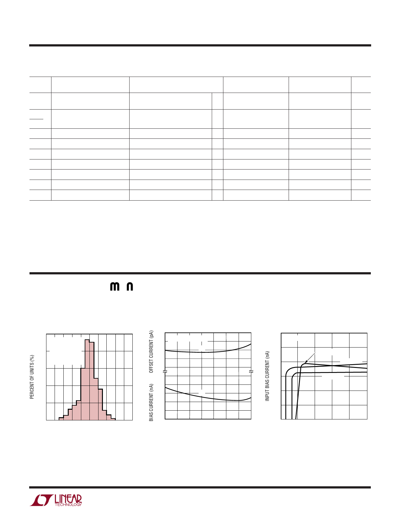
TYPICAL PERFORMANCE CHARACTERISTICS
Distribution of Offset Voltage
Drift with Temperature
25
VS = 5V, 0V
VCM = 0.1V
20 80 LT2078'S
25 LT2079'S
= 260 OP AMPS
15
10
5
0
–2
–1
0
1
2
OFFSET VOLTAGE DRIFT WITH TEMPERATURE (µV/°C)
LT2078/79 • TPC01
Input Bias and Offset Currents vs
Temperature
100
VS = 5V, 0V TO ±15V
50
IOS
0
–5
IB
–6
–7
–50 –25
0 25 50 75 100 125
TEMPERATURE (°C)
LT2078/79 • TPC02
Input Bias Current vs
Common Mode Voltage
0
VS = 5V, 0V
–2
TA = 125°C
–4
TA = –55°C
–6
TA = 25°C
–8
–10
–12
–1
0
1
2
3
4
COMMON MODE VOLTAGE (V)
LT2078/79 • TPC03
20789fa
5
Share Link: 