NCS2002 데이터 시트보기 (PDF) - ON Semiconductor
부품명
상세내역
제조사
NCS2002 Datasheet PDF : 16 Pages
| |||
NCS2002, NCV2002
CT
1.0 nF
0.9 V
R1a
470 k
R1b
470 k
RT
470 k
0.9 V
−
+
R2
470 k
fO = 1.5 kHz
Output Voltage
Timing Capacitor
Voltage
VCC
0
0.67 VCC
0.33 VCC
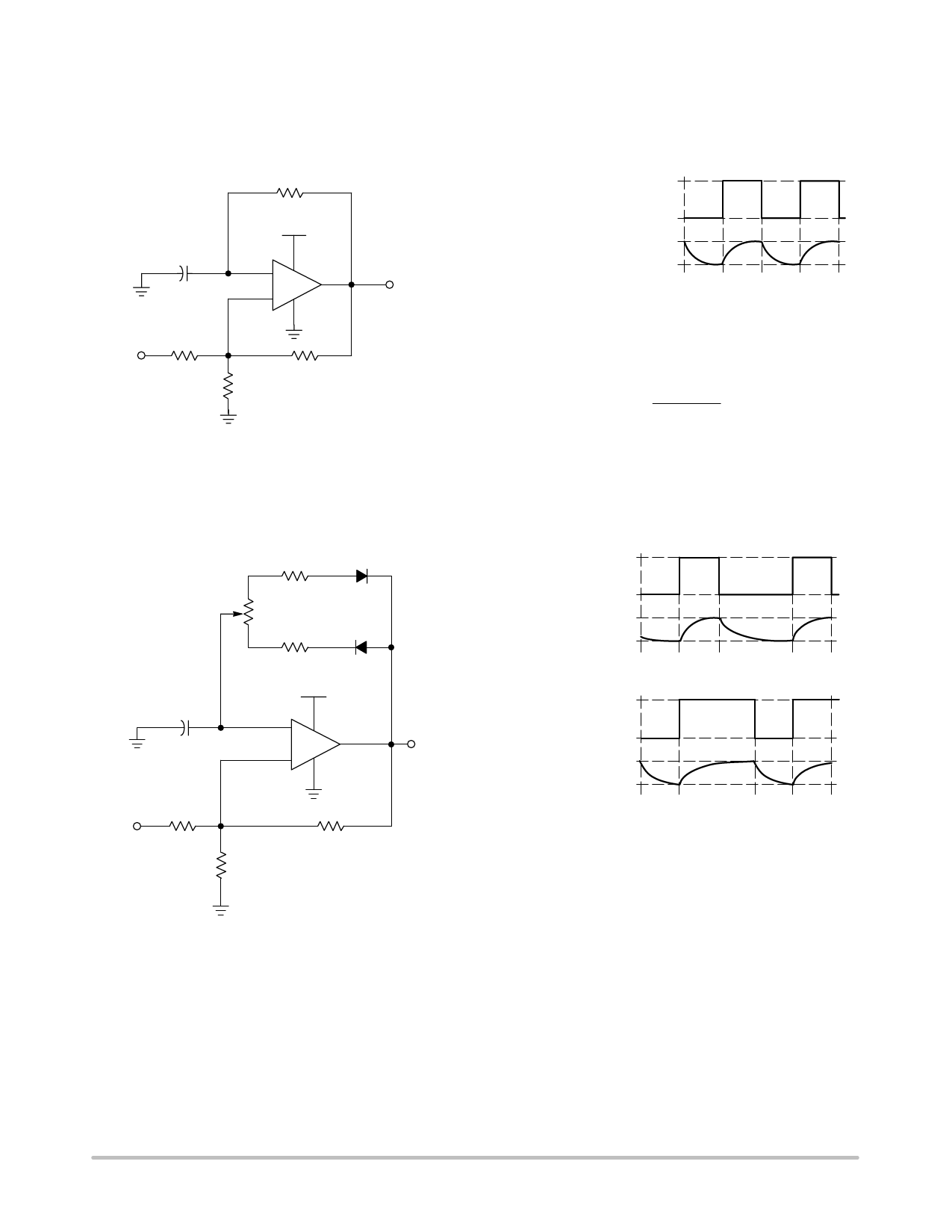
The non−inverting input threshold levels are set so that
the capacitor voltage oscillates between 1/3 and 2/3 of
VCC. This requires the resistors R1a, R1b and R2 to be of
equal value. The following formula can be used to
approximate the output frequency.
fO +
1.39
1
RTCT
Figure 37. 0.9 V Square Wave Oscillator
cww 10 k
D1
1N4148
1.0 M
cw
CT
1.0 nF
D2
10 k
1N4148
VCC
−
+
VCC
R1a
470 k
R1b
470 k
R2
470 k
Output Voltage
Timing Capacitor
Voltage
VCC
0
0.67 VCC
0.33 VCC
Clock−wise, Low Duty Cycle
VCC
Output Voltage
fO
0
Timing Capacitor 0.67 VCC
Voltage 0.33 VCC
Counter−Clock−wise, High Duty Cycle
The timing capacitor CT will charge through diode D2 and discharge
through diode D1, allowing a variable duty cycle. The pulse width of the
signal can be programmed by adjusting the value of the trimpot. The ca-
pacitor voltage will oscillate between 1/3 and 2/3 of VCC, since all the
resistors at the non−inverting input are of equal value.
Figure 38. Variable Duty Cycle Pulse Generator
http://onsemi.com
13
Share Link: 