UPC3224TB 데이터 시트보기 (PDF) - California Eastern Laboratories.
부품명
상세내역
제조사
UPC3224TB Datasheet PDF : 14 Pages
| |||
UPC3224TB
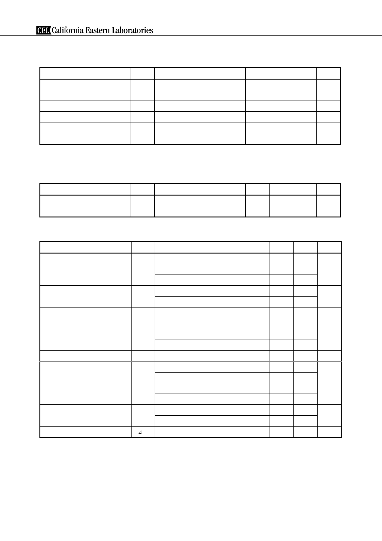
ABSOLUTE MAXIMUM RATINGS
Parameter
Supply Voltage
Total Circuit Current
Power Dissipation
Operating Ambient Temperature
Storage Temperature
Input Power
Symbol
Conditions
VCC TA = +25°C
ICC
TA = +25°C
PD TA = +85°C
TA
Tstg
Pin
TA = +25°C
Note
Ratings
6.0
25
270
−40 to +85
−55 to +150
+10
Unit
V
mA
mW
°C
°C
dBm
Note Mounted on double-sided copper-clad 50 × 50 × 1.6 mm epoxy glass PWB
RECOMMENDED OPERATING RANGE
Parameter
Supply Voltage
Operating Ambient Temperature
Symbol
VCC
TA
Conditions
MIN. TYP. MAX. Unit
4.5
5.0
5.5
V
−40
+25
+85
°C
ELECTRICAL CHARACTERISTICS (TA = +25°C, VCC = 5.0 V, ZS = ZL = 50 Ω)
Parameter
Circuit Current
Power Gain
Saturated Output Power
Gain 1 dB Compression Output
Power
Noise Figure
Upper Limit Operating Frequency
Isolation
Input Return Loss
Output Return Loss
Gain Flatness
Symbol
Test Conditions
ICC No input signal
GP f = 1.0 GHz, Pin = −30 dBm
f = 2.2 GHz, Pin = −30 dBm
PO (sat) f = 1.0 GHz, Pin = −5 dBm
f = 2.2 GHz, Pin = −5 dBm
PO (1 dB) f = 1.0 GHz
f = 2.2 GHz
NF f = 1.0 GHz
f = 2.2 GHz
fu 3 dB down below flat gain at f = 0.1 GHz
ISL f = 1.0 GHz, Pin = −30 dBm
f = 2.2 GHz, Pin = −30 dBm
RLin f = 1.0 GHz, Pin = −30 dBm
f = 2.2 GHz, Pin = −30 dBm
RLout f = 1.0 GHz, Pin = −30 dBm
f = 2.2 GHz, Pin = −30 dBm
∆GP f = 0.1 to 2.2 GHz
MIN.
7.0
19.0
18.5
+1.5
−1.5
−6.5
−8.5
−
−
2.8
35.0
37.0
9.0
10.0
11.0
8.0
−
TYP.
9.0
21.5
21.5
+4.0
+1.5
−3.5
−5.5
4.3
4.3
3.2
40.0
42.0
12.0
14.0
17.0
12.0
±0.8
MAX.
12.0
24.0
24.5
−
−
−
−
5.8
5.8
−
−
−
−
−
−
−
−
Unit
mA
dB
dBm
dBm
dB
GHz
dB
dB
dB
dB
4
Data Sheet PU10490EJ01V0DS
Share Link: 